Employing couplers to convert guided waves into free-space modes and flexibly control their wavefront is one of the key technologies in chip-integrated displays and communications. Traditional couplers are mainly composed of gratings, which have limitations in footprint, bandwidth, as well as controllability. Though the resonant/geometric metasurface newly emerges as a promising interface for bridging guided waves with free-space ones, it either relies on complex optimizations of multiple parameters, or is subject to the locked phase response of opposite spins, both of which hinder the functional diversity and practical multiplexing capability. Here, we propose and experimentally demonstrate an alternative with a spin-decoupled meta-coupler, simultaneously integrating triple functions of guided wave radiation, polarization demultiplexing, and dual-channel wavefront manipulation into a single device. By endowing polarization-dependent functionalities into a pure geometric metasurface, the out-coupled left-handed and right-handed circular polarization guided waves intelligently identify the predesigned phase modulation and reconstruct desired wavefronts, like bifocal focusing and holography multiplexing, with a polarization extinction ratio over 13.4 dB in experiments. We envision that the robust, broadband, and multifunctional meta-coupler could pave a way for the development of versatile multiplexed waveguide-based devices.
1. INTRODUCTION
Combining various functional optical devices, such as lasers, waveguides, modulators, and multiplexers/demultiplexers, into a photonic integrated circuit is of great significance to achieve versatile optical chips [1,2]. According to the different processes of controlling electromagnetic waves, the functions of photonic integrated devices can be roughly divided into three categories, including optical coupling [3], guided wave modulation [4], and guided wave radiation [5]. In particular, converting guided waves into free-space modes and manipulating their wavefront has a plethora of applications in light detection and ranging (LiDAR) [6], augmented reality/virtual reality displays [7], optical communications and optical interconnections [8], etc. Currently, mature guided wave radiators are based on grating couplers, which have limitations in bandwidth and functionalities, and lack complete control of scattered electromagnetic waves. Moreover, due to the existence of high-order diffraction, the footprint of the device is too large for the working wavelength, and it inevitably suffers from loss.
Fortunately, benefitting from the rapid development of nano-fabrication technology in recent years, the metasurface has emerged as a new platform for light manipulation at the subwavelength scale [9–13]. As an artificially designed electromagnetic interface, the metasurface is composed of subwavelength optical antennas, which allows flexible control over electromagnetic field properties, including amplitude, phase, and polarization. Apart from controlling the wavefront of light propagating in free space, the metasurface also has been recently integrated with waveguides for valuable application scenarios, varying from on-chip light coupling [14,15], polarization/mode sorting [16–19], mode routing [20,21], mode conversion [22,23], to frequency conversion [24].
Nevertheless, employing a metasurface to couple the guided wave into free space and conveniently manipulate the extracted waves in a desired way is still in its infancy [25–32]. For instance, off-chip beam deflection and focusing was first demonstrated by exploiting the collective resonant behavior of a metasurface patterned on a waveguide [25,26]. However, such a process of finding structures to cover the phase shift range imposed by the resonant principle is challenging, accompanied with relatively low robustness to the fabrication and small operation bandwidth. Subsequently, an identical metasurface with detour phase was constructed to flexibly mold the guided wave into free-space optical modes for holographic projections, but at an expense of complicated algorithm optimization to define the positions of meta-atoms [27,28]. As an alternative, we previously developed an interface of geometric metasurface based on the Pancharatnam–Berry (PB) phase, providing an easily implemented and highly versatile platform for bridging a link between guided waves and free-space functional beams [29,30]. Despite the geometric metasurface being robust, broadband, and easy to fabricate, it should be noted that there are fundamental symmetry restrictions between two circularly-polarized wave phases, hindering the functional diversity and multiplexing capability in the previous design. For example, if a focusing phase profile is designed with respect to a radiated left-handed circular polarization (LCP) wave, it turns to divergent for the right-handed circular polarization (RCP) wave, indicating only half part of the extracted guided wave can be utilized for functions by a pure geometric meta-coupler. On the other hand, with the increase of information transmission capacity, independent control of the wavefronts of spin light enables practical applications in a multiple-target detection radar/LiDAR system and multiple-input multiple-output communications [33,34]. Therefore, further research on spin light manipulation by couplers is highly expected and (de)multiplexing technology based on integrated waveguide may be more worthy of attention.
Sign up for Photonics Research TOC. Get the latest issue of Photonics Research delivered right to you!Sign up now
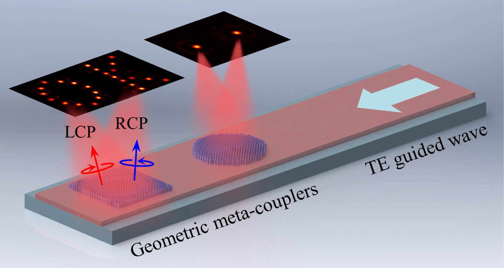
In this work, we extend the capability of the geometric metasurface and demonstrate a new meta-coupler to mold the guided wave radiation for multiplexing functionalities. Circumventing the joint modulated metasurface (PB phase combined with resonant phase, propagation phase, or detour phase) [35,36], a spin-decoupled geometric meta-coupler based on the pure PB phase is ingeniously proposed and experimentally validated. When directly driven by an eigen transverse electric (TE) mode, the meta-coupler converts it into LCP and RCP free-space waves, respectively, and realizes polarization-dependent focusing and holography multiplexing, as conceptually shown in Fig. 1. Distinguished from the previously demonstrated spin-decoupled metasurface, in which the incoming and output waves are both free-space light, ours bridges the guided modes and free-space waves, and it can simultaneously realize triple functions of guided wave coupling, polarization demultiplexing, and dual-channel wavefront manipulation in a single device. The robust and broadband coupler with a single configuration in controlling the guided wave radiation is expected to open a new perspective for constructing multifunctional guided-wave-driven devices and integrated systems.
Figure 1.Schematic plot of spin-decoupled meta-couplers endowed with triple functions of guided wave radiation, polarization demultiplexing, and dual-channel wavefront manipulation. Propagating guided waves interact with the geometric metasurfaces and are scattered out with polarization-dependent wavefronts simultaneously for two different specific functions, e.g., off-chip bi-focusing, dual-channel holography multiplexing.
Our earlier work revealed that the geometric metasurface composed of anisotropic meta-atoms with identical shapes and different in-plane orientations can be directly driven by an eigen-TE guided mode [29]. Here, as shown in Fig. 2, in analogy to linear polarized waves, a traveling TE guided wave (assumed to propagate along the direction) can be regarded as a superposition of LCP and RCP waves, carrying with phase of , where is the initial reference phase and is the propagation accumulated phase. Therefore, rotation of a meta-atom (orientation angle of ) will induce a PB phase () for the scattered LCP wave, followed by an opposite phase shift () for the RCP wave. The polarization behaviors and phase responses of all the scattered spatial waves are concluded as follows:
Figure 2.Illustration of the working principle of the spin-decoupled geometric meta-coupler excited by the TE guided mode. The traveling TE mode can be decomposed into the combination of LCP and RCP waves, respectively, both of which are coupled out and independently manipulated by the elaborately designed geometric metasurface with different phase profiles for function multiplexing.
For the geometric metasurface, only two parts and possess the additional PB phase, while the other two parts and do not carry any phase shift imposed by the metasurface. Once we arrange the meta-atoms with the appropriate period, such as less than half of the effective wavelength of the driven mode, then both the unmodulated waves ( and ) will not be coupled out due to the mismatched wave vector condition. As a result, the rest two parts (with phase shifts) can be simultaneously manipulated to achieve polarization-demultiplexed free-space functions with strategical designs. Specifically, if the geometric metasurface can simultaneously modulate extracted LCP and RCP waves to generate both RCP and LCP target light fields, the total phase profile and rotation angle of each meta-atom could be endowed as follows: where , and are the amplitude and required target phase profile for the scattered LCP wave and RCP wave, respectively. It should be noted that the total phase requirements in Eq. (2) contain two independent phase profiles: one is the phase profile that can convert the extracted RCP component into the LCP target light field, while the other is the phase profile that can convert the extracted LCP component into the RCP target light field. Therefore, the scattered LCP/RCP waves will “intelligently identify” the predesigned phase modulation and then reconstruct the target light field with different polarizations. Hence, a spin-decoupled meta-coupler with predesigned functions is realized by embedding two polarization-dependent functionalities into a pure geometric metasurface.
3. FUNCTION DEMONSTRATIONS
As a proof-of-concept demonstration of our proposed scheme on guide wave radiation manipulation by a spin-decoupled geometric meta-coupler, we first numerically and experimentally demonstrate off-chip polarization-demultiplexed focusing on a two-dimensional (2D) slab waveguide. Then, we also present a multiplexed holographic projection for a more general manifestation. Considering that there has been rapid growth in developing versatile photonic integrated devices based on lithium niobate (LN) especially after the birth of lithium niobate on insulator (LNOI) [37,38], it has excellent optoelectronic properties, involving a wide low-loss optical transparency window, large second-order nonlinear coefficient, and large electro-optic coefficient. Here we take it as an ideal waveguide platform for investigations and applications.
A. Meta-Coupler for Off-Chip Polarization-Demultiplexed Focusing
Starting from a simple case, we consider a TE guided mode propagating along the direction inside a -cut LN slab waveguide, whose thickness is 300 nm, with a 1.8-μm-thick silica () layer as the substrate. The fundamental TE mode has a propagation constant and has a plane wavefront in the direction, where is the wave vector in free space. We then put the geometric meta-coupler made of amorphous silicon () metasurface on top of the slab waveguide, the unit of which has a length , width , and height . To eliminate the undesired scattering of the CP light without PB phase, the period of the metasurface is fixed at half of the effective wavelength of the TE mode. Here, Si is an optimal material to construct the metasurface antennas since it has a large refractive index in contrast with LN, and the fabrication technology is well-developed. Moreover, it has a negligible material loss in the telecommunication wavelength range and has been maturely employed for plentiful high-quality integrated devices. It should also be emphasized that we do not intentionally optimize the geometry parameters of the Si nanorod since the PB phase response is robust and easy to implement, the only influence of which is on the guide-wave extraction efficiency. By calculation in our model, an up-extraction efficiency of per nanorod is around 0.08%.
Specifically, we design the meta-coupler to perform as a 2D bi-focusing metalens. The scattered LCP wave is supposed to be focused at one focal point (, , ), while the RCP wave is focused to another focal point (, , ). The required phase profile for each metalens should fulfill the parabolic function as below: In order to reduce the demand for computational resources, we demonstrate a small meta-coupler in full-wave simulations, performed by a finite-difference time-domain solver (FDTD Solutions, Lumerical). For details, μ, μ, μ, μ, μ, and μ. The diameter of the meta-coupler is 15 μm and the designed numerical aperture (NA) is around 0.3. From Eqs. (2) and (3), we obtain the orientations of the nanorods and construct the meta-coupler. The corresponding simulation results are then illustrated in Fig. 3. Figures 3(a)–3(c) depict the electric-field intensity distribution in the plane, where the TE mode is injected into the slab waveguide from its left port and propagates through the metasurface region. It evanescently couples with the nanorods of the metasurface and a small portion of it is extracted into free space with different polarizations imposed with different phase lags. The simulation results indicate that the scattered LCP light is focused on a focal spot at (, 0, 25.3) μm above the slab waveguide, and the scattered RCP light is focused on another spot at (4.95, 0, 25.3) μm simultaneously, matched the theoretical designs. Such meta-coupler structures actually cause a small perturbation to the guided mode, and the mode distortion analysis is also carried out in Appendix A. Then the electric-field intensity distributions at the focal plane are exhibited in Figs. 3(d)–3(f). For a quantitative analysis of the focusing characteristics, we calculate the full width at half-maximum (FWHM) of the two focal spots, manifesting about 2.92 μm () in the direction and 2.76 μm () in the direction for LCP light, and about 2.87 μm () in the direction and 2.70 μm () in the direction for RCP light, which means the focused beam has a near-diffraction-limited spot size (2.6 μm, ) in the simulation [Figs. 3(g) and 3(h)]. In addition, we calculate the polarization extinction ratio (PER) to quantitatively analyze the polarization demultiplexing performance of the meta-coupler, which is defined as the ratio of the electric-field intensities of the two orthogonal polarization components at the focus point: in which and are the electric-field intensity of the LCP and RCP components, respectively. When μ, the intensity of the LCP component reaches the maximum, and the PER is 19.2 dB; when μ, the intensity of the RCP component reaches the maximum, and the PER is 19.7 dB. Furthermore, considering the PB phase is robust to the wavelength, the bandwidth analysis is also conducted in Appendix B.
Figure 3.Numerical simulation of meta-coupler enabled off-chip polarization-demultiplexed focusing. The light propagates along the axis from left to right as the red arrow shown. Scattered light intensity distribution in the plane of the (a) LCP component, (b) RCP component, (c) total field. Light intensity distribution at the focal plane of the (d) LCP component, (e) RCP component, (f) total field. Intensity distribution along the (g) direction and (h) direction at the focal plane, indicating the focused beam has a near-diffraction-limited spot size. The PER at the LCP focal point and RCP focal point is evaluated at 19.2 dB and 19.7 dB.
Afterward, we fabricate the polarization-demultiplexed meta-coupler in experiment using electron beam lithography (EBL, ELS-F125, Elionix) and inductively coupled plasma reactive ion etching (ICP-RIE, HSE200, Naura) to define the metasurface patterned on the LNOI slab waveguide (see Appendix C). The scanning electron microscopy (SEM) images of the fabricated metasurfaces are shown in Figs. 4(a) and 4(b). The metasurface region has a diameter μ, and the designed two focal positions are (, 0, 80) μm and (20, 0, 80) μm, respectively, whose NA keeps the same as the simulations. Then a home-built optical setup (see Appendix D) is implemented to characterize the performance of the waveguide integrated metalens. The intensity distribution at the focal plane for LCP and RCP light together with the total field is measured individually and demonstrated in Figs. 4(c)–4(e). We also map the intensity distribution at the cross-section, as shown in Fig. 4(f). As expected, our experimental results show a similar intensity distribution profile to that in simulations, indicating two focal points at (, 0, 79) μm and (17.9, 0, 79) μm, with LCP and RCP, respectively. The FWHMs of the LCP focal spot are around 3.61 μm (, direction) and 3.7 μm (, direction), while the FWHMs of the RCP focal spot are around 4.15 μm (, direction) and 3.57 μm (, direction), which are slightly larger than the theoretically predicted. The experimental PER at the LCP focal point and RCP focal point is also evaluated around 15.2 dB and 13.4 dB [Figs. 4(g) and 4(h)].
Figure 4.Experimental demonstration of polarization-demultiplexed focusing by a meta-coupler based on an LNOI waveguide. (a) SEM image of the fabricated Si metasurface dressed on the LNOI slab waveguide. (b) Zoom-in SEM image of the details of the metasurfaces. (c)–(e) Measured intensity distribution of the LCP component, RCP component, and total field at the focal plane. (f) Reconstructed total intensity distribution in the propagation plane. (g), (h) Intensity distribution of the LCP and RCP waves along the and directions at the focal plane. The PER at each focal point is 15.2 dB and 13.4 dB.
B. Meta-Coupler for Multiplexed Hologram Generation
More generally, by leveraging the ability to control the phase profile of scattered guided wave by the meta-coupler, a dual-channel multiplexed holographic projection is also theoretically and experimentally manifested. The holograms here are calculated by the point-source algorithm for simplicity [27]. By individually deriving the required phase profile of the letters “O” and “K,” and mapping the total phase profile into the spin-decoupled meta-coupler, a polarization-demultiplexed holographic generator is completed with well-designed simulations and experiments. Such a hologram device has a footprint of μμ and produces two images at a distance of 80 μm. The simulation results are shown in Figs. 5(a)–5(c), where each field distribution is obtained by the vector diffraction method of the near field at μ calculated by FDTD. It can be clearly seen that the target holographic images with different polarizations are successfully reproduced through our design method. The experimental images are also reconstructed under the excitation of the TE mode of 1550 nm, agreeing well with the simulated results [Figs. 5(d)–5(f)].
Figure 5.Simulated and experimentally constructed holographic images of the dual-channel multiplexing meta-coupler. (a), (d) The holographic images of the letter “O” with LCP, which are reproduced at μ. (b), (e) The holographic images of letter “K” with RCP reproduced at the same plane. (c), (f) The superposed two images with orthogonal polarization.
Generally, the polarization conversion efficiency (PCE) is essential in traditional free-space geometric metasurface designs. Since a small PCE means less scattered light flips their spins with phase shift for manipulation, and it will degrade the modulation efficiency, meanwhile bring more noise to the signal, scanning of a large number of parameters to achieve the desired metasurface unit for high PCE is inevitable. But in our waveguide system, by controlling the wave vector matching condition, the guided wave without phase shift will keep propagating inside the waveguide and then interact with the rest of the nanorods. The total efficiency is not related to the PCE, and it maintains a high signal-to-noise ratio for guided wave manipulation. Therefore, we do not need to specially optimize the geometry parameters of the metasurface for its robustness of phase response against size and material property variations. In addition, integrating our geometric meta-couplers with the LNOI waveguide offers a versatile platform for future dynamic devices. Attributed to the distinctive electro-optic property of LN, chip integrated dynamic displays, communications, light detection, and ranging could be expected.
In summary, we have demonstrated a spin-decoupled meta-coupler with pure geometric metasurface, simultaneously realizing triple functions of guided wave radiation, polarization demultiplexing, and dual-channel wavefront manipulation in a single device. The meta-coupler converts the TE guided wave into LCP and RCP free-space waves, respectively, and realizes polarization-dependent functions. A set of design scenarios using Si antennas-patterned LN waveguides is successively demonstrated in simulations and experiments at the telecommunication wavelength, including multiplexed focusing and hologram generation. Our developed meta-coupler has advantages in the simplicity of manipulating guided wave radiation (design without scanning a large number of parameters or complex algorithm optimization) and functional diversity (multiplexing technology), promising a plethora of multifunctional chip-integrated devices.
APPENDIX A: GUIDED MODE DISTORTION ANALYSIS
In our designs, we ensure the distortion to a negligible degree. The thickness of the LNOI slab waveguide is 300 nm, which only supports two modes ( and ). The simulated real part of the electric field across the meta-coupler region inside the waveguide is shown in Fig. 6(a); it shows a small distortion, manifesting that the metasurface we employed here induces negligible mode conversion inside the waveguide. By conducting a mode decomposition for the guided wave after the metasurface in Fig. 6(b), we find that the transmitted field merely has fundamental mode (transmission intensity ). Since the period of the metasurface along the propagation direction is designed to be half wavelength of the guided wave, it inevitably generates backward Bragg reflection with a reflection intensity of around 22.2%, which can be eliminated by further decreasing the period. Meanwhile, the effective impedance difference between the meta-coupler and the waveguide region will also affect the reflection property as well as the far-field scattering, which can be tuned by the structure of the PB unit [39–42]. Therefore, we can assume that the presence of the meta-coupler has only a small perturbation to the guided modes.
Figure 6.(a) Real part of the guided wave electric field underneath the meta-coupler region shows small distortion. (b) Transmission intensity for different modes after the metasurface region. Only the fundamental mode is detected at the end of the waveguide.
Validated by full-wave simulations (Fig. 7), the polarization-demultiplexed metalens can perform in a wavelength range beyond 600 nm (1250–1850 nm). In principle, the scattered local phase of the metasurface decorated on the waveguide accumulates from the propagation phase of the guided wave and PB phase of the metasurface. Though the PB phase is robust to the wavelength, the dispersion effect of the guided wave propagation phase and diffraction dispersion of the lens phase profile still works. As a result, the beam spot will shift and distort when the wavelength changes. In addition, high-order diffractions gradually emerge in the shorter wavelength range, which further deteriorates the focusing performance.
APPENDIX C: SAMPLE FABRICATION
The samples were fabricated on a commercially available LNOI wafer (available in NANOLN Company) with a 300-nm-thick LN device layer and 1.8 μm buried silicon dioxide (Fig. 8). It was first cleaned with sonication in acetone and dried with a stream, followed by deposition of 300-nm-thick by plasma-enhanced chemical vapor deposition. Subsequently, the meta-coupler and grating patterns were defined by the EBL process (ELS-F125, Elionix) on a positive electron beam resist (PMMA). After development, a chromium (Cr) layer was deposited using electron-beam evaporation, followed by lift-off to transfer the patterns. Then the Cr layer served as a hard mask for dry etching the Si layer in a mixture of and plasma (HSE200, Naura). Finally, the remaining Cr mask was removed by ammonium cerium nitrate.
APPENDIX D: OPTICAL SETUP FOR MEASUREMENTS
Schematic of the optical setup used for characterizing the performance of the meta-couplers is shown in Fig. 9. A continuous-wave tunable laser (Fianium supercontinuum) is coupled into the slab waveguide by a grating coupler to excite the fundamental TE mode, assisted with a linear polarizer and an objective ( magnification, NA = 0.7). The scattered-out light by the meta-coupler is collected by another objective ( magnification, NA = 0.42), and then passes through the polarization analyzer (a quarter-wave plate combined with a linear polarizer) and lens before projecting into an infrared camera (Xenics Xeva 1083) for imaging. Since the objective for collection is mounted on a translational stage with an actuator in the direction, we can record the light field at different propagation distances by 2D real-space images, and then reconstruct a 3D volumetric image by stacking the 2D images.
APPENDIX E: POLARIZATION DEMULTIPLEXING WITH GEOMETRIC META-COUPLERS IN A STRIP WAVEGUIDE
Since the strip (or ridge) waveguide is widely applied in integrated photonics, here we also make an investigation on one-dimensional (1D) light field phase manipulation in the LNOI strip waveguide. In our paradigm, the LN waveguide has a height and width μ, the Si antenna has a length , width , and height . The center-to-center distance between the adjacent nanorods is 300 nm, and the footprint of the meta-coupler is 29.4 μm. A mode of 1550 nm () is input from the left port, and the extracted LCP light converges at one focal point above the waveguide, while the RCP wave converges at another focal point. The simulated total intensity distributions are shown in Fig. 10.
Figure 10.1D light field manipulation by the spin-decoupled geometric meta-coupler in a strip waveguide. e.g., polarization-demultiplexed metalens is implemented with full-wave simulation.