Achromatic Talbot lithography (ATL) with high resolution has been demonstrated to be an excellent technique for large area periodic nano-fabrication. In this work, the uniformity of pattern distribution in ATL was studied in detail. Two ATL transmission masks with ~50% duty cycle in a square lattice were illuminated by a spatial coherent broadband extreme ultraviolet beam with a relative bandwidth of 2.38%. Nonuniform dot size distribution was observed by experiments and finite-difference time-domain simulations. The sum of the two kinds of diffraction patterns, with different lattice directions (45° rotated) and different intensity distributions, results in the final nonuniform pattern distribution.
Two-dimensional (2D) ordered nanostructures have received considerable attention in recent years due to their unique properties and potential applications in biosensors[1], optical displays[2], microelectronics and optoelectronics[3,4], metamaterials[5–7], etc. Various techniques such as electron-beam (e-beam) lithography (EBL)[8], nano-imprinting lithography[9], interference lithography (IL) by laser[10–12], nanosphere lithography[13,14], chemical synthesis, and self-assembly[15] have been utilized to fabricate large area, high resolution nanostructures with tunable dimensions and properties. These conventional lithography techniques have some more or less drawbacks. For instance, EBL is with high cost and low throughput, nano-imprinting has problems in resist adhesion, and self-assembly chemical synthesis is difficult to obtain uniform dot size. Laser-induced surface patterning[16,17] was also used for large area periodic nanoarray fabrication. However, low precision, simple product structure, and special substrate material dependence limit its real applications. High resolution and large area periodic nanostructures are still an enormous challenge for all of these techniques.
In recent years, extreme ultraviolet (EUV) IL technology has been developed to fabricate high resolution periodic nanopatterns over large areas[18–22]. The throughput of the EUV-IL technique is much higher than that of those traditional lithography methods. Line structures with a 6 nm half-pitch (HP), which is the record in photon-based lithography, have been afforded in the EUV-IL beamline at the Paul Scherrer Institute (PSI)[19]. In this technique, a transmission-grating type of multi-gratings mask is employed. Periodic nanostructures are formed by the interference of the first or second order diffracted beams from the multi-gratings mask. The period of the interference pattern () produced by two-beam EUV-IL can be expressed as where is the wavelength, is the diffraction angle of the th-order diffraction beam, and is the period of the grating. Thus, the resolution limit of EUV-IL is about one half of the working wavelength (), and the depth of focus (DOF) of EUV-IL should be , where is the side length of the grating. The drawbacks of this technique are the difficulty in controlling the duty cycle of the patterned nanostructures and the limited patterned area, which is much smaller than the illuminated area during exposure.
In 1836, Talbot observed the coherent self-imaging property of a periodic grating[23]. This effect was mathematically explained in 1881 by Rayleigh[24]. Under the illumination of a monochromatic light source, stationary self-images of a one-dimensional (1D) periodic grating will happen at multiples of the Talbot distance (), which can be calculated as where is the wavelength, and is the period of the grating structure. Based on the self-imaging effect, Talbot lithography under monochromatic illumination has been used for imaging processing and synthesis, optical testing, spectrometry, and periodic complex patterns fabrication over large areas[25–29]. However, the very limited DOF requires very precise positioning of the distance from the sample to the mask, which makes this technique difficult to use for large area nanostructures fabrication.
Sign up for Chinese Optics Letters TOC. Get the latest issue of Chinese Optics Letters delivered right to you!Sign up now
Under the broadband illumination with a spectral bandwidth, Guerineau et al. found that achromatic and stationary patterns of a 1D periodic grating can be obtained behind the distance where is the relative spectral bandwidth of the source[30]. This was called the achromatic Talbot effect. It should be noted that the stationary patterns beyond are a result of interference of all diffraction orders from the same grating. As the distance of the sample plane from the mask increases, the diffraction orders diverge from each other, and the patterned area approaches zero at the maximum distance [31,32]. For a grating with a side length of , can be expressed as
Thus, the DOF of achromatic Talbot lithography (ATL) should be
To obtain a large DOF, the relationship of and should be
ATL, also known as achromatic spatial frequency multiplication (ASFM), has also been developed to fabricate large area high resolution nanostructures with a large DOF[31–35]. In this technique, a single-grating mask is employed, which enables full use of the illuminated area. All of the diffraction waves through the mask contribute to the resulted pattern with high contrast and sharp intensity profile. In general, the resolution of the pattern is limited by the resolution of the mask. Writing dense, periodic structures using EBL and electroplating of the dense structures is not so easy. The minimum period of features patterned by ATL is 70 nm with 15 nm dot size[34]. The theoretical limit approaches a 7.5 nm HP by using 10.9 nm EUV light[36]. Superior uniformity was emphasized in all of the above high resolution ATL results. However, for the square lattice mask with duty cycle, a nonuniform dot size distribution was found[37]. The question is whether the nonuniform dot size distribution can only be found for the square lattice mask with a smaller duty cycle.
In this Letter, the pattern uniformity in the usual 50% duty cycle ATL exposure was further explored. Nonuniform dot size distribution was observed after ATL exposure at the X-ray IL (XIL) beamline in the Shanghai Synchrotron Radiation Facility (SSRF) for the gold masks in the square lattice with 50% duty cycle. Finite-difference time-domain (FDTD) analysis revealed that the sum of the two kinds of diffraction patterns, with different lattice directions (45° rotated) and different intensity distributions, results in the final nonuniform pattern distribution.
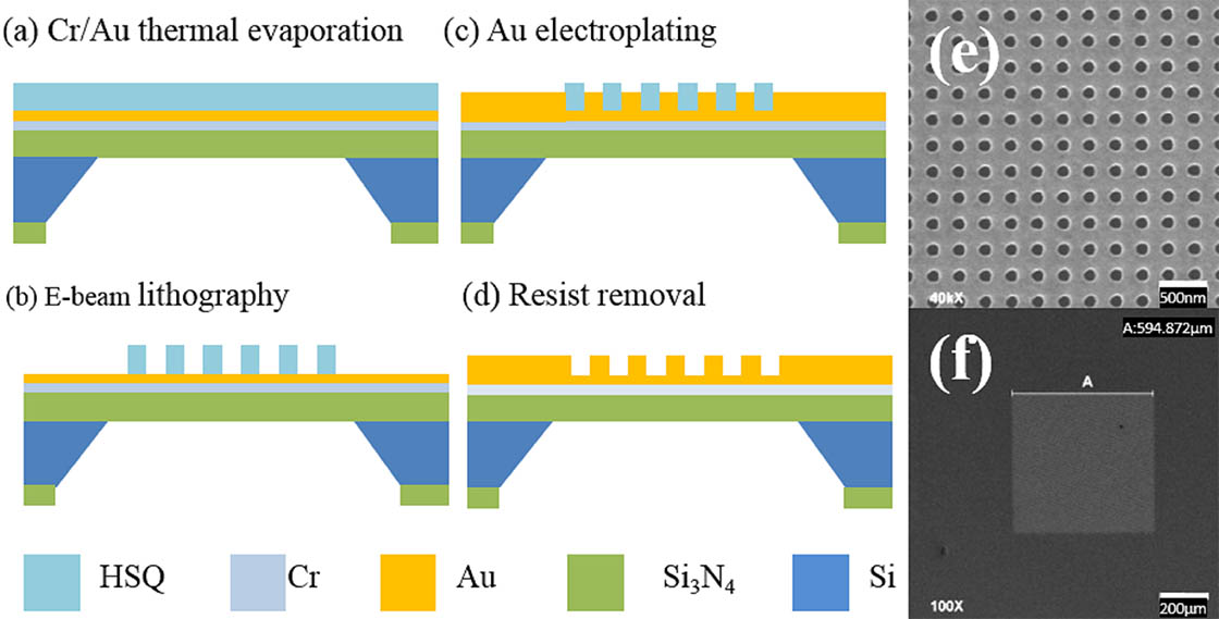
Two pieces of square lattice masks with 50% duty cycle, fabricated by EBL followed by the Au electroplating process, have been exposed at the XIL beamline in SSRF. The scheme of the mask fabrication process is shown in Figs. 1(a)–1(d). A 4 nm thick Cr adhesion layer and a 8 nm thick Au seed layer were deposited onto a 100 nm thick membrane by an e-beam evaporation system, Mantis Qprep. After that, hydrogen silsesquioxane (HSQ, XR1541-006) was spin-coated onto the Au layer at 4000 r/min and prebaked at 180°C for 5 min with a thickness of , as shown in Fig. 1(a). 2D periodic HSQ pillar arrays in a square lattice were then written by an EBL system (Crestec CABL-9000 C) at 50 keV, as shown in Fig. 1(b). After being developed in tetramethylammonium hydroxide (TMAH)-25% for 60 s, rinsed in deionized (DI) water, and dried with nitrogen, the HSQ pillar arrays were transferred into the Au layer with a thickness of 60 nm by the electroplating process, as shown in Fig. 1(c). The Au electroplating process is similar to that reported by Xie et al. and Liu et al.[38,39]. To obtain a smooth Au layer with a smaller grain size, the sodium Au sulfite solution ( concentration, Elevate Gold 7990, Technic, Inc.) was used at with 10% duty cycle bipolar pulses. After being electroplated in Elevate Gold 7990 at 42°C for 10 min, a 60 nm thick Au layer was electroplated onto the HSQ pillar arrays. Finally, the membrane with HSQ pillar arrays and the Au layer were rinsed in 1% hydrofluoric acid (HF) for 30 s to remove the HSQ resist, and 2D transmission masks with 280 and 600 nm pitch and 50% duty cycle were fabricated over an area of , as shown in Fig. 1(d). The scanning electron microscopy (SEM) images of the fabricated masks with 280 nm pitch are presented in Figs. 1(e) and 1(f).
Figure 1.(a)–(d) Schematic illustrations of the mask fabrication process by the Au electroplating process, SEM images of the 2D hole mask with (e) 280 nm pitch and (f) an area of . Scale bars for (e) and (f) correspond to 500 nm and 200 μm.
The masks described above were exposed at the XIL branch beamline (BL08U1B) of SSRF, China[20]. By using a 4.2 m long Apple-II-type elliptically polarized undulator (EPU), the energy range of XIL can be arranged from 85 to 150 eV with a relative bandwidth of 2.38% (). The beamline layout has been described elsewhere in detail[20]. For the ATL exposure, a central wavelength of 13.5 nm was arranged by adjusting the EPU gap distance. By prebaking at 180°C for 5 min, HSQ (XR1541-002)-coated silicon wafers with a thickness of were used for exposure. After exposure, the wafers were developed in TMAH-25% for 60 s and rinsed in DI water. To check the smallest feature size, the exposure dose was varied between 150 and with a step dose.
For the mask with a 280 nm pitch, SEM images of the exposed samples at 0.48 mm () and 1.5 mm beyond the mask are shown in Figs. 2(a) and 2(b). A uniform pattern distribution in a 198 nm pitch was detected at 0.48 mm. The smallest feature size of was detected with a dose, as shown in Fig. 2(a). At the working distance of 1.5 mm, a nonuniform pattern distribution with a two-dot size of 56 and 46 nm was detected in a 198 nm pitch, as shown in Fig. 2(b). For the mask with the 600 nm period, SEM images of the exposed samples at 2.24 mm () and 4.5 mm beyond the mask are shown in Figs. 2(c) and 2(d). Nonuniform pattern distribution in a 424 nm pattern pitch was detected. As shown in Fig. 2(c), 89 and 70 nm size dots were obtained at 2.24 mm at a dose of . The dot sizes were 102 and 96 nm at the working distance of 4.5 mm, as shown in Fig. 2(d).
Figure 2.SEM images of the fabricated square nanopatterns with 198 nm period at (a) 0.48 mm and (b) 1.5 mm with a dose of . Scale bars for (a) and (b) are equal to 200 nm. SEM images of the fabricated square nanopatterns with 424 nm period at (c) 2.24 mm and (d) 4.5 mm with a dose of . Scale bars for (c) and (d) are equal to 500 nm.
A commercial FDTD software (Lumerical Solutions, Inc.) was used to simulate the aerial electrical field intensity distribution behind the masks. FDTD has been used to simulate the Talbot effect of a high density grating[40]. In this Letter, an example from the Application Gallery of Lumerical was used for the far field electrical field intensity calculation[41]. The mask structures used in the simulation are the same as that described above. Au nanohole arrays with 280 and 600 nm pitch (P), 50% duty cycle (D/P), and a thickness of 60 nm were put on a 100 nm thick membrane, as shown in Fig. 3. The dielectric constants for Au and were from the Center for X-Ray Optics (CXRO) database[42]. A plane Gaussian wave with a central wavelength of 13.5 nm and a relative bandwidth of 2.38% was normally illuminated on the two masks.
Figure 3.(a) Illustration of the three-dimensional graph of the mask structure. A 60 nm thick Au layer with 50% duty cycle was put on a 100 nm membrane. (b) Illustration of the 2D graph of the mask structure. (c) Illustration of the side view of the mask structures with period P and hole diameter D.
For the 2D periodic arrays in the square and hexagonal lattices, the electrical field intensity distribution under normal illumination was proved to be polarization independent[37]. Thus, only the results under TM polarized radiation are presented here. A 0.5 nm mesh grid was used. Periodic boundary conditions in the and directions and perfect matched layer (PML) boundary conditions in the direction were applied during the simulation. It should be noted here that during FDTD, the electrical field intensity distribution can only be done for one monochromatic wavelength at a time. To obtain the total electrical field intensity distribution under a Gaussian plane wave, the contributions of various wavelengths to the final electrical field intensity distribution were calculated separately and then summed up according to their spectral weight of histograms[36]. In order to achieve stable results, the broadband Gaussian spectrum, with a central wavelength of 13.5 nm and a relative bandwidth of 2.38%, has to be approximated with a sufficient number of monochromatic waves, the spectral weight of which equals their histogram intensity ratio in the total broadband Gaussian spectrum. Correspondingly, in this work, 101 wavelengths with 0.01 nm steps were used as the broadband spectrum.
Figure 4 shows the calculation results for the two square lattice masks under TM polarization radiation. For the mask with a 280 nm pitch, the aerial images generated at 0.488 mm () and 1.5 mm behind the mask are illustrated in Figs. 4(a) and 4(b). The aerial images generated from another square lattice mask with 600 nm pitch are illustrated in Figs. 4(e) and 4(f) at 2.24 mm () and 4.5 mm behind the mask. The profiles of the electrical field intensity distribution along the white dashed lines in Figs. 4(a), 4(b), 4(e), and 4(f) are shown in Figs. 4(c), 4(d), 4(g), and 4(h). For the two masks, the calculated images show a pattern period equal to the mask period divided by , shown in Figs. 4(a), 4(b), 4(e), and 4(f). A uniform pattern distribution with the same maximum intensity along the diagonal line is shown in Figs. 4(a) and 4(c) for the mask with the 280 nm pitch at . While nonuniform pattern distributions with different maximum intensities along the diagonal line are shown in Figs. 4(b), 4(e), 4(f) and 4(d), 4(g), 4(h), this is very different from other results, in which superior uniformity was always emphasized in the high resolution periodic nanopatterns fabrication[31–35].
Figure 4.Calculated images for the mask with 280 nm pitch at (a) 0.488 mm and (b) 1.5 mm. Calculated images for the mask with 600 nm pitch at (e) 2.24 mm and (f) 4.5 mm. (c), (d) and (g), (h) Profiles of electrical field intensity distribution along the white dashed lines in (a), (b) and (e), (f), respectively.
The simulation results in Fig. 4 were consistent with the exposure results in Fig. 2. Nonuniform square patterns with different maximum intensity distributions with the period being equal to the mask period divided by were both obtained by the experimental and simulation results. The nonuniform square pattern generation was explained by detailed FDTD analysis. It should be noted here that during FDTD, the electrical field intensity distribution can only be done for one monochromatic wavelength at a time. To obtain the total electrical field intensity distribution under a Gaussian plane wave, the contributions of various wavelengths, , were calculated separately, and the total electrical field intensity distribution under a Gaussian plane wave, , was achieved by summing up the contributions of the different wavelengths according to their spectral weight[36], which means where the subscript is the central wavelength, 101, and is the spectral weight of the monochromatic wavelength of in the simulated Gaussian plane wave. For detailed explanation of the summing results of the different wavelengths, the square lattice mask with the 600 nm pitch was simulated at 4.5 mm, shown in Fig. 5. Figure 5(a) shows the electric field intensity distribution under a monochromatic illumination of 13.51 nm. Figure 5(b) shows the electric field intensity distribution under a monochromatic illumination of 13.59 nm. The two patterns show different positions for the maximum intensity, which are 45° rotated and non-rotated relative to the mask symmetry in Fig. 3(b). Similar with the monochromatic 2D fractional Talbot effect[43], a half-period shift in the and directions in the 45° rotated pattern was observed. For the total electrical field intensity distribution under the broadband EUV beam, the intensity of the patterns with the same symmetry as that in Fig. 5(a) was added together according to their spectral weight, and the resulted 45° rotated pattern was shown in Fig. 5(c). The sum of the intensity of patterns like that in Fig. 5(b) led to the non-rotated pattern in Fig. 5(d). The patterns in Figs. 5(c) and 5(d) show different maximum intensities. The accumulation of Figs. 5(c) and 5(d) resulted in the final total nonuniform electrical field intensity distribution under the broadband EUV beam, as shown in Fig. 4(f).
Figure 5.(a), (b) Two representative monochromatic electrical field intensity distributions for the square lattice mask with 600 nm period at 4.5 mm. (c), (d) The sum of those two group patterns with the same symmetry as that in (a) and (b).
In fact, according to the detailed FDTD analysis, the patterns under broadband EUV illumination can be classified into two groups, non-rotated patterns and the 45° rotated patterns relative to the mask symmetry. The patterns in the same group are added up according to their spectral weight. The final pattern distribution under the broadband EUV beam is the total sum of the two group patterns, the intensities of which are usually different. Thus, nonuniform final pattern distribution will be obtained. However, if the intensities of the two group patterns are approximately equal, uniform final pattern distribution will be obtained. We also obtained uniform pattern distribution for the mask with the 280 nm pitch at 0.48 mm beyond the mask.
In summary, the ATL pattern uniformity was experimentally and theoretically investigated for two square lattice masks with 50% duty cycle. Both uniform and nonuniform pattern distributions were obtained at the XIL branch beamline in SSRF. Detailed FDTD analysis showed that the sum of the two kinds of diffraction patterns, with different lattice directions (45° rotated and non-rotated relative to the mask), results in the final pattern distribution. If the two group pattern intensities are equal, uniform pattern distribution can be obtained. If the two group pattern intensities are really different, nonuniform final pattern distribution can be obtained. It is necessary to conduct FDTD analysis before the ATL experiment.