• Photonics Research
  • Vol. 10, Issue 9, 2261 (2022)
Tomáš Halenkovič1、3、*, Magdaléna Kotrla1, Jan Gutwirth1, Virginie Nazabal1、2, and Petr Němec1、4、*
Author Affiliations
  • 1Department of Graphic Arts and Photophysics, Faculty of Chemical Technology, University of Pardubicehttps://ror.org/01chzd453, Pardubice, Czech Republic
  • 2Univ Rennes, CNRS, ISCR (Institut des Sciences Chimiques de Rennes)–UMR 6226, F-35000 Rennes, France
  • 3e-mail: tomas.halenkovic@upce.cz
  • 4e-mail: petr.nemec@upce.cz
  • show less
    DOI: 10.1364/PRJ.460552 Cite this Article Set citation alerts
    Tomáš Halenkovič, Magdaléna Kotrla, Jan Gutwirth, Virginie Nazabal, Petr Němec. Insight into the photoinduced phenomena in ternary Ge-Sb-Se sputtered thin films[J]. Photonics Research, 2022, 10(9): 2261 Copy Citation Text show less

    Abstract

    The kinetics of photoinduced changes, namely, photobleaching and photodarkening in sputtered ternary Ge29Sb8Se63 thin films, was studied. The study of time evolution of the absorption coefficient Δα(t) upon room-temperature near-bandgap irradiation revealed several types of photoinduced effects. The as-deposited films exhibited a fast photodarkening followed by a dominative photobleaching process. Annealed thin films were found to undergo photodarkening only. The local structure studied by Raman scattering spectroscopy showed significant structural changes upon thermal annealing, which are presumably responsible for a transition from the photobleaching observed in as-deposited and reversible photodarkening in annealed thin films. Moreover, a transient photodarkening process was observed in both as-deposited and annealed thin films. The influence of the initial film thickness and laser optical intensity on the kinetics of photoinduced changes is discussed.

    1. INTRODUCTION

    Photostructural changes in amorphous chalcogenide thin films and chalcogenide glasses have been extensively studied for many decades [1]. The chemical bond rearrangement induced by light excitation having energy near the bandgap of these materials leads to the modifications of the amorphous matrix, resulting in changes of optical properties [2]. These are referred to as photodarkening (PD) and photobleaching (PB), depending on the sign of the change [3]. The magnitude of PD and PB is related to the composition and structure of chalcogenide materials. While in binary arsenic-based chalcogenides only PD occurs, both germanium-based binaries [4,5] and ternaries show rather complex behavior with the sign of the change being a product of the competitive processes of PD and PB [6,7].

    The PD of exposed annealed films of As2S3 and As2Se3 that may be partially recovered by the consequent annealing was reported as early as the 1970s by De Neufville et al. [1]. It is considered that as-deposited amorphous chalcogenide thin films possess irreversible photoinduced changes, while annealed films and melt-quenched glasses undergo reversible ones [8]. Recently, a waveguide inscription using femtosecond lasers [ultrafast laser inscription (ULI)] attracted the attention of some researchers [9,10]. This process includes the nonlinear absorption of sub-bandgap light, resulting in changes in the refractive index. Results on ULI in Ge-Sb-S glasses by means of structural studies suggest that the driving forces of PD during ULI in chalcogenide glasses are of the same origin as photostructural changes due to the near-bandgap continuous-wave laser irradiation [10]. A better comprehension of the processes and variables involved in photoinduced phenomena may play an important role for potential applications, optimization, and tailoring properties of these materials in the fields of photonic integrated circuits, holographic gratings, and waveguide inscription [11].

    The aim of this paper is to provide a study of photoinduced changes in Ge-Sb-Se chalcogenide thin films, which are of particular interest in the field of photonic integrated circuits for their potential application in nonlinear optics [12] and optical sensors in the mid-infrared domain [13,14]. The nominal composition of Ge25Sb10Se65 was chosen based on our previous work related to a photosensitivity study on this system [15]. It combines favorable optical properties and expected photosensitivity. Relatively high optical bandgap energy causes the orange color of thin films within the range of thicknesses under study, which in combination with low surface reflectivity allows easy detection of photoinduced changes. The insight into the photoinduced changes provided in this paper summarizes up to date available references and tries to recognize the challenges in understanding the general principles of these phenomena. The influence of thickness and the laser optical intensity on the kinetics of these processes is discussed.

    2. METHODS

    A sputtering target (ø=50  mm) of Ge25Sb10Se65 chalcogenide glass was synthesized by a melt-quenching technique described elsewhere [16]. Thin films with thicknesses d of 350, 500, and 650 nm were deposited by rf-sputtering (13.56 MHz) at 5×10³  mbar working pressure of argon onto well-cleaned microscope slides (soda-lime float glass, substrate length of 76 mm). The variance in the thickness was estimated to be <6% within the substrate length. Selected thicknesses were found to be optimal for our experiments, as the penetration depths of the pump laser described below are 700 and 1800  nm for as-deposited and annealed films, respectively.

    The composition of thin films was verified by energy-dispersive X-ray spectroscopy (EDS) with a scanning electron microscope (JEOL IT-300, JEOL Ltd., Japan). X-ray diffraction (XRD) patterns were collected within the range of 2θ from 10° to 80° with a step of 0.02° (Cu Kα, Rigaku, Japan). Thicknesses of the thin films and their initial optical properties, specifically, refractive index n and optical bandgap energy Eg, were determined from variable angle spectroscopic ellipsometry (VASE, J. A. Woollam, USA).

    Annealing of samples was performed at a temperature of 250°C (i.e., glass transition temperature of bulk Tg50°C) for 2 h (heating rate of 2°C·min1, cooling rate of 1°C·min1) under an argon atmosphere.

    The kinetics of photoinduced changes of both as-deposited and annealed samples at room temperature was studied by means of in situ transmittance measurements captured by a fiber-coupled high-resolution spectrometer (OceanInsight, USA). Samples were placed in a hermetically sealed cell equipped with quartz windows filled with pure argon gas and irradiated by near-bandgap light coming from a 589 nm (2.1 eV) continuous-wave diode-pumped solid state (DPSS) laser source (Shanghai Laser & Optics Century Co., Ltd., China) for 180 min. The experimental setup for in situ kinetics measurements is depicted in Fig. 1(a). To retain the athermal nature of photoinduced changes, low to moderate laser optical intensities, specifically, 3.0±0.5, 19.0±2.5, 50.0±3.0, and 125±5.0  mW·cm2, were used.

    (a) Experimental scheme of irradiation setup for in situ measurements. A pump beam from a DPSS laser is aimed onto the sample through the plano–convex lens, and its desired optical intensity is adjusted by the neutral density filter(s) (ND). (b) Typical time evolution of absorption coefficient Δα(t) for as-deposited film (black) and annealed film (red) upon room-temperature irradiation at laser optical intensity of 125 mW·cm−2; shaded region represents the data acquisition after the laser is switched off; insets with photodarkened (top) and photobleached (bottom) University of Pardubice logo using 1 mm diameter negative stencil (colors are illustrational only without profiling).

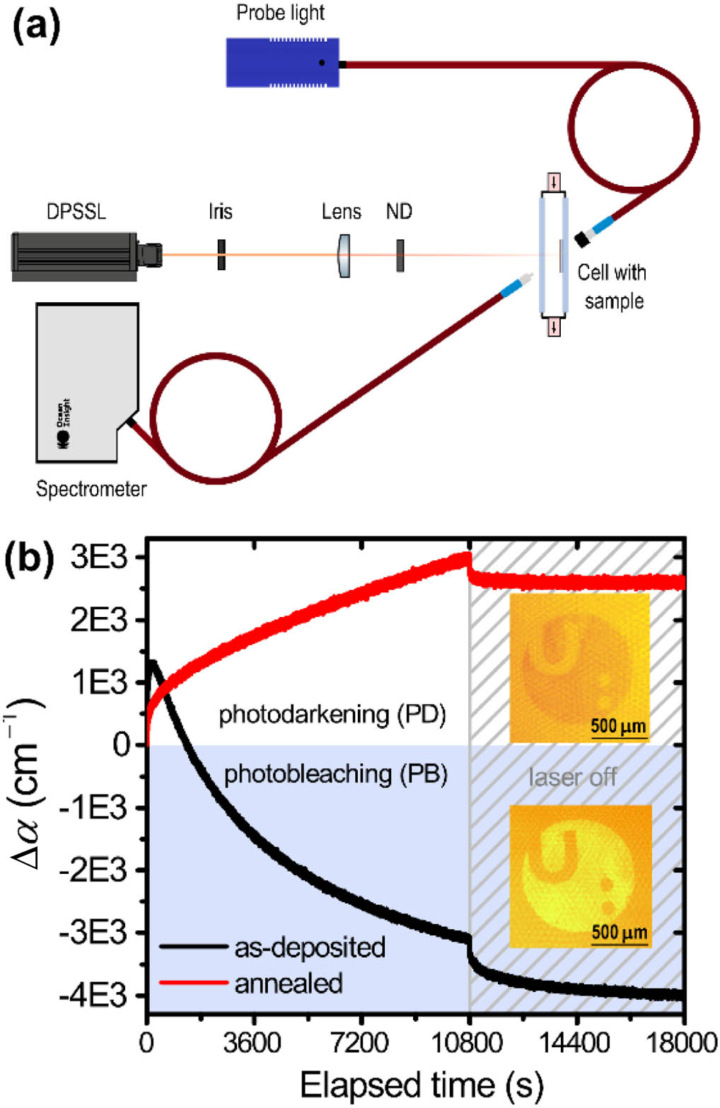
    Figure 1.(a) Experimental scheme of irradiation setup for in situ measurements. A pump beam from a DPSS laser is aimed onto the sample through the plano–convex lens, and its desired optical intensity is adjusted by the neutral density filter(s) (ND). (b) Typical time evolution of absorption coefficient Δα(t) for as-deposited film (black) and annealed film (red) upon room-temperature irradiation at laser optical intensity of 125  mW·cm2; shaded region represents the data acquisition after the laser is switched off; insets with photodarkened (top) and photobleached (bottom) University of Pardubice logo using 1 mm diameter negative stencil (colors are illustrational only without profiling).

    The changes were expressed as the time evolution of the absorption coefficient Δα(t) calculated as Δα(t)=ln[T0·T(t)1]·d1, where T0 is the initial transmittance, and T(t) is the transmittance at elapsed time t. The selected value of the initial transmittance at irradiation wavelength was 18%, corresponding to the region of exponential absorption edge (Urbach edge, at initial value of absorption coefficient α of order of 104  cm1). It is worth to note that the small changes in thickness are expected during irradiation (such as photoinduced volume change in As2S3 chalcogenide glass [17]); however, this does not affect the value of Δα significantly. Changes in reflectance during irradiation were also neglected.

    The magnitude of the absorption edge shift by means of a change of Eg succeeding irradiation was determined directly from transmittance measurements using WVASE32 software (J. A. Woollam, USA). It should be emphasized that the evaluation of the absolute values of Eg and its changes was not the target of this work, and so the precision of the estimation using this approach is rather coarse with expected accuracy of about ±0.02  eV. Potential changes in local structure upon thermal annealing and irradiation were examined by a μ-Raman spectrometer (LabRam HR800, Horiba Jobin-Yvon, USA) coupled with a 100× microscope (Olympus, Japan).

    3. RESULTS AND DISCUSSION

    A. Optical Properties of Thin Films

    The chemical composition of the vitreous target was found to be Ge24Sb11Se66 (±1%, atomic fraction). In agreement with a previous work on this system [16], slight changes in stoichiometry during the sputtering process were observed, as the composition of thin films was Ge29Sb8Se63 (±1%, atomic fraction). The optical bandgap energy Eg of as-deposited thin films was 1.87±0.02  eV, and the refractive index n at 1550 nm was 2.55±0.01 as determined by VASE using a Cody–Lorentz oscillator model. An annealing treatment caused bleaching of thin films, resulting in an optical bandgap energy increase to 1.96±0.02  eV accompanied by a slight refractive index decrease to 2.54±0.01. Both as-deposited and annealed ones were found to be amorphous according to XRD measurements.

    As shown in Fig. 1(b), the prolonged irradiation caused the change of an opposite sign, i.e., PB in as-deposited films and PD in annealed ones, reasonably of the highest magnitude when the laser optical intensity of 125  mW·cm2 was used. It should be noted that even after 3 h of irradiation, the photoinduced change was not fully saturated, and so for measurements at lower laser optical intensities, the irradiation time was conserved.

    The highest magnitude of PB by means of an increase in Eg of about 0.04±0.02  eV was found in the sample with a thickness of 350  nm. On the other hand, the highest measure of PD, specifically, the decrease in Eg by 0.05±0.02  eV, was found in the sample with a thickness of 650  nm under the abovementioned conditions.

    B. Millisecond Kinetics of Photoinduced Changes

    The study of the time evolution of the absorption coefficient Δα(t) revealed several types of photoinduced effects. First, as-deposited films exhibit fast PD, which is entirely dominated by PB in the long term. Such behavior has already been observed in some as-deposited selenide films, e.g., in evaporated GeSe2 [18] and Ge-As-Se [7], pulsed laser deposited Ge-Sb-Se [19], or in cosputtered Ga-Sb-Se [20]. Moreover, only PD takes place during the irradiation of annealed films. Finally, a transitory change, specifically, transient PD (TPD), was observed in both as-deposited and annealed thin films.

    As seen in Fig. 2 (top panel), PB in as-deposited thin films is strongly thickness dependent, having the magnitude of a process indirectly proportional to the thickness. It is worth to note that the PB effect in the film with a thickness of 350  nm (violet curve) is closest to being saturated when irradiated by 125  mW·cm2 laser optical intensity. Presumably, the observed PB effect upon prolonged near-bandgap irradiation is of a similar origin to the bleaching upon thermal annealing. Such a change comes from a mutual polymerization of defective entities resulting in ordered structures via homo- to heteropolar bond conversion [1]. The excitation generates the charged radiation defects followed by recombination-induced bond rearrangements due to the diffusion of atoms [21]. Although the photoexcited states have not yet been proven experimentally [22], their existence leading to an increased short- and medium-range order [23] is a generally accepted explanation of irreversible changes in different properties including an absorption edge shift. Other stabilization mechanisms, such as void collapsing [22], evaporation of volatile entities, and photo-enhanced oxidation [24], may contribute to these changes. Because the experiments performed in this work were carried out in a pure argon atmosphere, we do not expect that the latter has an important contribution to the observed effects.

    Time evolution of absorption coefficient Δα(t) of as-deposited (top panel) and annealed (bottom panel) Ge-Sb-Se thin films upon room-temperature irradiation depending on thicknesses (in nm) at different laser optical intensities varying from 3 to 125 mW·cm−2.

    Figure 2.Time evolution of absorption coefficient Δα(t) of as-deposited (top panel) and annealed (bottom panel) Ge-Sb-Se thin films upon room-temperature irradiation depending on thicknesses (in nm) at different laser optical intensities varying from 3 to 125  mW·cm2.

    In contrast with PB observed in as-deposited thin films, the PD in annealed thin films as seen in Fig. 2 (bottom panel) is proportionally dependent on the thickness and is a universal process observed in annealed chalcogenide glasses and thin films, i.e., reversible PD effect, which may be recovered by thermal annealing. The mechanism of reversible changes is not yet known, as no subtle structural changes have yet been experimentally determined. They are likely the result of a similar elemental process to the irreversible ones, i.e., recombination-induced bond rearrangements and atom motions [3]. Presumably, the reversible PD comes from valence band broadening, resulting in a redshift [22].

    The origin of fast PD in as-deposited films is not yet fully understood. Sati and Jain [6] proposed that it originates in homo- to heteropolar bond conversion at deformed sites such as Se–Se dimers at the [GeSe4/2] or Sb–Sb bonds caused by Sb–Sb–Se in defective [SbSe3/2] pyramidal units, present in evaporated Ge-Sb-Se thin films, and is simply a competitive process to slow PB, which becomes dominant in the long term. Relative to time, the magnitude of PB is rather small compared to PD.

    Besides being thickness dependent, fast PD and slow PB in as-deposited and reversible PD in annealed Ge-Sb-Se thin films are strongly dependent on laser optical intensity as depicted in Figs. 3(a) and 3(b), respectively. The time evolution of fast PD shows a saturation at 125  mW·cm2 within 245  s and clearly delays with decreasing intensity. A similar observation was reported for evaporated Ge-As-Se films by Khan et al. [25]. The process of fast PD becomes completely dominated by the slow PB process.

    (a) Time evolution of absorption coefficient Δα(t) of as-deposited and (b) annealed Ge-Sb-Se thin films with thickness of ∼650 nm depending on the laser optical intensity. (c) On/off cycle (240 s) experiment with as-deposited (black line) and annealed (red line) Ge-Sb-Se thin films with the same thickness using laser optical intensity of 50 mW·cm−2. The shaded area corresponds to the cycle when the laser is switched on.

    Figure 3.(a) Time evolution of absorption coefficient Δα(t) of as-deposited and (b) annealed Ge-Sb-Se thin films with thickness of 650  nm depending on the laser optical intensity. (c) On/off cycle (240 s) experiment with as-deposited (black line) and annealed (red line) Ge-Sb-Se thin films with the same thickness using laser optical intensity of 50  mW·cm2. The shaded area corresponds to the cycle when the laser is switched on.

    Transitory changes by means of TPD were easily noticed by the on/off experiments in Fig. 3(c). TPD has already been observed by various authors [7,19,2629] and may be related to a phenomenon termed as an “optical stopping effect” by Matsuda et al. in the 1970s [30]. Ganjoo et al. [27] observed TPD in annealed evaporated amorphous selenium a-Se and As2Se3 of 500  nm thickness when the film was irradiated by an Ar ion laser (λ=514  nm, optical intensity of 80  mW·cm2). An apparent rise in the transmittance after switching the laser off (λ=488 and 660 nm, 150  mW·cm2) was also reported for 1 μm thick as-deposited GeSe2 and Ge2Se3 evaporated films by Yan et al. [28]. A similar behavior was found in sputtered as-deposited Ge-As-Se thin films at different intensities when the films were exposed to a 655 nm laser diode [29]. Additionally, the magnitude of TPD among the references herein seems to be affected by the optical intensity and metastable PD or PD, depending on composition. The structural origin of TPD is yet to be understood. In situ extended X-ray absorption fine structure (EXAFS) experiments on amorphous selenium indicate that it may be associated with a chalcogen coordination number increase upon irradiation [22,31].

    Finally, the results on millisecond kinetics of photoinduced changes in as-deposited and annealed Ge-Sb-Se thin films suggest that they are of the very same origin as in the Ge-As-Se system [29]. Even though the sign and the magnitude of a change may differ with composition and structure [5,7,15], the TPD and reversible PD in annealed thin films seem to be a universal feature of photoinduced changes in amorphous chalcogenides.

    C. Structural Changes upon Annealing and Irradiation

    Changes in local structure upon thermal annealing and irradiation were investigated using Raman scattering spectroscopy measurements. As depicted in Fig. 4, the Raman spectra of Ge-Sb-Se thin films are prima facie dominated by the band peaking at 199  cm1, which corresponds to A1 symmetric stretching vibrations of heteropolar Ge–Se bonds in a corner-sharing [GeSe4/2] tetrahedron. The companion mode A1C assigned to edge-sharing tetrahedral units is located at 214  cm1 [32]. The overlapping E1 mode of [SbSe3/2] pyramidal units around 191  cm1 may contribute to the Raman intensity of the A1 mode [33]. The peak around 174  cm1 is considered to come from Ge–Ge homopolar bonds in ethane-like [Ge2Se6/2] units [34]. Vibrational modes of Sb–Sb in [Se2SbSbSe2] found at 160  cm1 probably contribute to this peak [35].

    (a) Normalized reduced intensity of Raman spectra of nonirradiated as-deposited and (b) nonirradiated annealed Ge-Sb-S thin films.

    Figure 4.(a) Normalized reduced intensity of Raman spectra of nonirradiated as-deposited and (b) nonirradiated annealed Ge-Sb-S thin films.

    To justify changes in structure, Raman spectra were deconvoluted using eight Gaussian peaks. Besides the five peaks mentioned above, the rotational modes in selenium polymeric chains (140  cm1 [35]) and bending vibrational modes of Se–Se at the outrigger (135145  cm1 [36]) are altogether represented by the Gaussian peak centered at 134  cm1. The A1 vibrational mode of Sen chains in amorphous selenium found at 235  cm1, stretching vibrational modes of Se–Se bonds at the outrigger (245  cm1), A1 vibrational modes of Se–Se dimers and short Sen chains in corner-linked [GeSe4/2], (260265  cm1 [35]), and Ge–Ge homopolar bonds’ vibrations coming from [GeGemSe4m (m=1, 2, 3, 4)], found at 270  cm1 [34] are collectively represented by Gaussian at 262  cm1. Finally, F1 asymmetric vibrational modes of GeSe4 tetrahedrons are found at 300  cm1 [32].

    Upon thermal annealing, an apparent change in the ratio between A1 (green) and A1C (blue) peaks occurred. A simultaneous decrease in the intensity of a peak centered at 134  cm1 (red) and 262  cm1 (orange) indicates the consumption of selenium atoms as a consequence of increased local order. Other noticeable changes occurred around the 174  cm1 peak. These changes may be due to a decrease in Ge–Ge homopolar bonds in ethane-like [Ge2Se6/2] units. Changes in intensity of surrounding peaks upon thermal annealing are low and difficult to justify.

    Photostructural changes by means of Raman scattering spectroscopy have already been described by several authors. The bond breaking mechanism upon irradiation followed by bond rearrangement and/or crystallization of structural sites is usually connected to changes in optical properties (i.e., shift of the absorption edge and refractive index changes upon irradiation) [4,7,37]. Being noteworthy, even in the highly photosensitive composition of As2S3, the fully saturated PD process results in only up to 1% of nearest neighbor bond alterations at available atomic sites [2]. As only low to moderate laser optical intensities were used in the present study, negligible changes in Raman spectra were observed and do not allow a fine analysis of the mechanisms involved.

    It can be assumed that the abovementioned structural changes upon thermal annealing are responsible for a transition from the PB observed in as-deposited and reversible PD in annealed Ge-Sb-Se thin films. In addition, although the experiments were carried out under a pure argon atmosphere, the photo-enhanced oxidation should not be completely ruled out from the contribution to the photoinduced changes, as the concentration of germanium is 29% (atomic fraction) [38].

    4. CONCLUSION

    A comprehensive study of photosensitivity in amorphous Ge29Sb8Se63 thin films by means of time evolution of the absorption coefficient Δα(t) revealed several types of photoinduced effects in these materials. Fast PD followed by a slow dominative PB process is present in as-deposited films, while only PD takes place during prolonged irradiation of annealed films. The structural changes upon thermal annealing seem to be responsible for a transition from the PB observed in as-deposited and reversible PD in annealed thin films. TPD was observed in both as-deposited and annealed thin films and, together with a PD in annealed films, seems to be a universal feature of photoinduced changes in amorphous chalcogenides. The processes behind metastable PD and PB in the as-deposited films as well as TPD, which seem to be associated with transitory photoexcited states, remain to be better understood. Furthermore, a thorough study of surface and thickness changes upon irradiation and annealing as well as long-term stability at normal room conditions in similar systems is also of interest. Such investigations may lead to the implementation of these materials and photonic processes in them in the design and engineering of photonic integrated circuits by means of tailoring and optimization of optical properties and inscription of three-dimensional structures (e.g., waveguides, holographic gratings, and diffractive optics elements).

    References

    [1] J. P. De Neufville, S. C. Moss, S. R. Ovshinsky. Photostructural transformations in amorphous As2Se3 and As2S3 films. J. Non-Cryst. Solids, 13, 191-223(1974).

    [2] S. Ducharme, J. Hautala, P. C. Taylor. Photodarkening profiles and kinetics in chalcogenide glasses. Phys. Rev. B, 41, 12250-12259(1990).

    [3] H. Fritzsche. The origin of reversible and irreversible photostructural changes in chalcogenide glasses. Philos. Mag. B, 68, 561-572(1993).

    [4] R. R. Kumar, A. R. Barik, E. M. Vinod, M. Bapna, K. S. Sangunni, K. V. Adarsh. Crossover from photodarkening to photobleaching in a-GexSe100–x thin films. Opt. Lett., 38, 1682-1684(2013).

    [5] T. Halenkovič, J. Gutwirth, T. Kuriakose, M. Bouška, M. Chauvet, G. Renversez, P. Němec, V. Nazabal. Linear and nonlinear optical properties of co-sputtered Ge-Sb-Se amorphous thin films. Opt. Lett., 45, 1523-1526(2020).

    [6] D. C. Sati, H. Jain. Coexistence of photodarkening and photobleaching in Ge-Sb-Se thin films. J. Non-Cryst. Solids, 478, 23-28(2017).

    [7] P. Khan, H. Jain, K. V. Adarsh. Role of Ge:As ratio in controlling the light-induced response of a-GexAs35−xSe65 thin films. Sci. Rep., 4, 4029(2014).

    [8] G. Pfeiffer, M. A. Paesler, S. C. Agarwal. Reversible photodarkening of amorphous arsenic chalcogens. J. Non-Cryst. Solids, 130, 111-143(1991).

    [9] A. Arriola, S. Gross, M. Ams, T. Gretzinger, D. Le Coq, R. P. Wang, H. Ebendorff-Heidepriem, J. Sanghera, S. Bayya, L. B. Shaw, M. Ireland, P. Tuthill, M. J. Withford. Mid-infrared astrophotonics: study of ultrafast laser induced index change in compatible materials. Opt. Mater. Express, 7, 698-711(2017).

    [10] G. Torun, A. Yadav, K. A. Richardson, Y. Bellouard. Ultrafast laser direct-writing of self-organized microstructures in Ge-Sb-S chalcogenide glass. Front. Phys., 10, 883319(2022).

    [11] A. Zakery, S. R. Elliott. Optical properties and applications of chalcogenide glasses: a review. J. Non-Cryst. Solids, 330, 1-12(2003).

    [12] E. Delcourt, N. Jebali, L. Bodiou, M. Baillieul, E. Baudet, J. Lemaitre, V. Nazabal, Y. Dumeige, J. Charrier. Self-phase modulation and four-wave mixing in a chalcogenide ridge waveguide. Opt. Mater. Express, 10, 1440-1450(2020).

    [13] M. Baillieul, E. Baudet, K. Michel, J. Moreau, P. Němec, K. Boukerma, F. Colas, J. Charrier, B. Bureau, E. Rinnert, V. Nazabal. Toward chalcogenide platform infrared sensor dedicated to the in situ detection of aromatic hydrocarbons in natural waters via an attenuated total reflection spectroscopy study. Sensors, 21, 2449(2021).

    [14] V. Mittal, G. Z. Mashanovich, J. S. Wilkinson. Perspective on thin film waveguides for on-chip mid-infrared spectroscopy of liquid biochemical analytes. Anal. Chem., 92, 10891-10901(2020).

    [15] T. Halenkovič, J. Gutwirth, P. Němec, E. Baudet, M. Specht, Y. Gueguen, J.-C. Sangleboeuf, V. Nazabal. Amorphous Ge-Sb-Se thin films fabricated by co-sputtering: properties and photosensitivity. J. Am. Ceram. Soc., 101, 2877-2887(2018).

    [16] F. Verger, V. Nazabal, F. Colas, P. Němec, C. Cardinaud, E. Baudet, R. Chahal, E. Rinnert, K. Boukerma, I. Peron, S. Deputier, M. Guilloux-Viry, J. P. Guin, H. Lhermite, A. Moreac, C. Compère, B. Bureau. RF sputtered amorphous chalcogenide thin films for surface enhanced infrared absorption spectroscopy. Opt. Mater. Express, 3, 2112-2131(2013).

    [17] K. Tanaka. Photoexpansion in As2S3 glass. Phys. Rev. B, 57, 5163-5167(1998).

    [18] A. R. Barik, R. Naik, K. V. Adarsh. Unusual observation of fast photodarkening and slow photobleaching in a-GeSe2 thin film. J. Non-Cryst. Solids, 377, 179-181(2013).

    [19] M. Olivier, R. Boidin, P. Hawlová, P. Němec, V. Nazabal. Kinetics of photosensitivity in Ge-Sb-Se thin films. International Conference on Photonics, Optics and Laser Technology (PHOTOPTICS), 61-66(2015).

    [20] T. Halenkovič, J. Gutwirth, M. Bouška, L. Calvez, P. Němec, V. Nazabal. Amorphous Ga–Sb–Se thin films fabricated by co-sputtering. Opt. Lett., 45, 29-32(2020).

    [21] Y. S. Kaganovskii, H. Genish, M. Rosenbluh. Laser recording in chalcogenide glass films: driving forces and kinetics of the mass transfer. Phys. Status Solidi A, 217, 2000523(2020).

    [22] K. Tanaka, K. Shimakawa. Light-induced phenomena. Amorphous Chalcogenide Semiconductors and Related Materials, 163-226(2021).

    [23] L. Tichý, V. Smrčka, H. Tichá, E. Sleeckx, P. Nagels. On the origin of photo-induced and thermally induced irreversible bleaching of amorphous Ge-Se films. Philos. Mag. Lett., 68, 73-79(1993).

    [24] C. A. Spence, S. R. Elliott. Light-induced oxidation and band-edge shifts in thermally evaporated films of germanium chalcogenide glasses. Phys. Rev. B, 39, 5452-5463(1989).

    [25] P. Khan, A. R. Barik, E. M. Vinod, K. S. Sangunni, H. Jain, K. V. Adarsh. Coexistence of fast photodarkening and slow photobleaching in Ge19As21Se60 thin films. Opt. Express, 20, 12416-12421(2012).

    [26] K. Shimakawa, Y. Ikeda. Transient responses of photodarkening and photoinduced volume change in amorphous chalcogenide films. J. Optoelectron. Adv. Mater., 8, 2097-2100(2006).

    [27] A. Ganjoo, K. Shimakawa, K. Kitano, E. A. Davis. Transient photodarkening in amorphous chalcogenides. J. Non-Cryst. Solids, 299–302, 917-923(2002).

    [28] Q. Yan, H. Jain, J. Ren, D. Zhao, G. Chen. Effect of photo-oxidation on photobleaching of GeSe2 and Ge2Se3 films. J. Phys. Chem. C, 115, 21390-21395(2011).

    [29] Z. Zhang, S. Xu, Y. Chen, X. Shen, R. Wang. Photo-induced effects in Ge-As-Se films in various states. Opt. Mater. Express, 10, 540-548(2020).

    [30] A. Matsuda, H. Mizuno, T. Takayama, M. Saito, M. Kikuchi. “Stopping effect” on guided light in As–S films by a laser beam. Appl. Phys. Lett., 24, 314-315(1974).

    [31] A. V. Kolobov, H. Oyanagi, K. Tanaka, K. Tanaka. Structural study of amorphous selenium by in situ EXAFS: observation of photoinduced bond alternation. Phys. Rev. B, 55, 726-734(1997).

    [32] P. Němec, B. Frumarová, M. Frumar. Structure and properties of the pure and Pr3+-doped Ge25Ga5Se70 and Ge30Ga5Se65 glasses. J. Non-Cryst. Solids, 270, 137-146(2000).

    [33] Z. G. Ivanova, E. Cernoskova, V. S. Vassilev, S. V. Boycheva. Thermomechanical and structural characterization of GeSe2–Sb2Se3–ZnSe glasses. Mater. Lett., 57, 1025-1028(2003).

    [34] K. Jackson, A. Briley, S. Grossman, D. V. Porezag, M. R. Pederson. Raman-active modes of a-GeSe2 and a-GeS2: a first-principles study. Phys. Rev. B, 60, R14985(1999).

    [35] M. Olivier, J. C. Tchahame, P. Němec, M. Chauvet, V. Besse, C. Cassagne, G. Boudebs, G. Renversez, R. Boidin, E. Baudet, V. Nazabal. Structure, nonlinear properties, and photosensitivity of (GeSe2)100-x(Sb2Se3)x glasses. Opt. Mater. Express, 4, 525-540(2014).

    [36] E. Baudet, C. Cardinaud, A. Girard, E. Rinnert, K. Michel, B. Bureau, V. Nazabal. Structural analysis of RF sputtered Ge-Sb-Se thin films by Raman and X-ray photoelectron spectroscopies. J. Non-Cryst. Solids, 444, 64-72(2016).

    [37] S. Zhang, Y. Chen, R. Wang, X. Shen, S. Dai. Observation of photobleaching in Ge-deficient Ge16.8Se83.2 chalcogenide thin film with prolonged irradiation. Sci. Rep., 7, 14585(2017).

    [38] L. Tichý, H. Tichá, K. Handlíř, K. Jurek. Photoinduced bleaching of Ge35S65 amorphous film. J. Non-Cryst. Solids, 101, 223-226(1988).

    Tomáš Halenkovič, Magdaléna Kotrla, Jan Gutwirth, Virginie Nazabal, Petr Němec. Insight into the photoinduced phenomena in ternary Ge-Sb-Se sputtered thin films[J]. Photonics Research, 2022, 10(9): 2261
    Download Citation