
Guoqing Chang, "New opportunities with an old optical material: an interview with Professor Marko Lončar," Adv. Photon. 4, 030503 (2022)
- Advanced Photonics
- Vol. 4, Issue 3, 030503 (2022)
Abstract
![]()
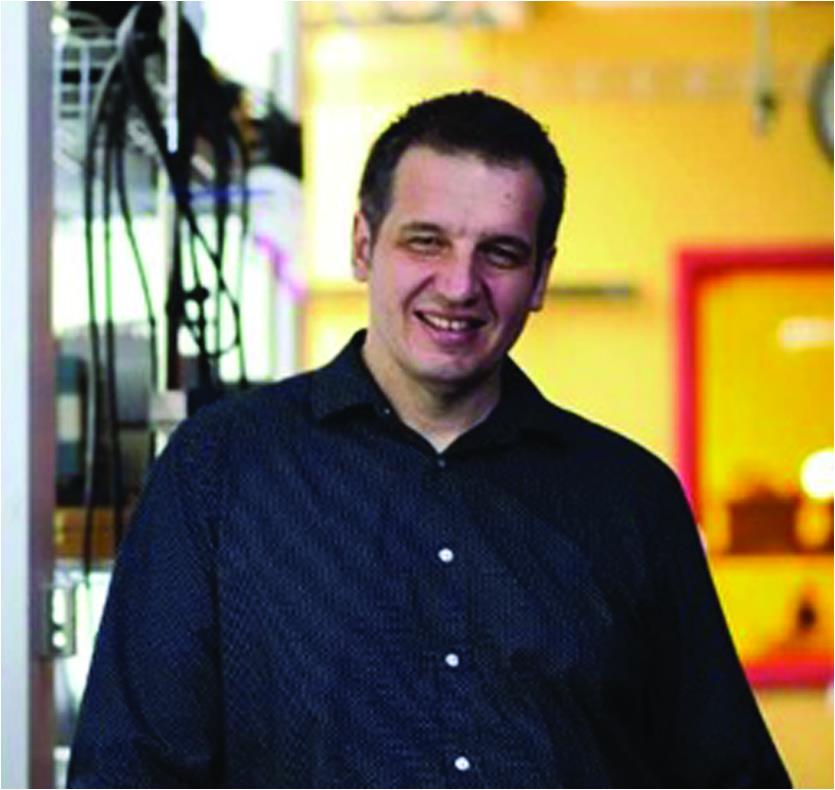
Figure 1.Marko Lončar, Tiantsai Lin Professor of Electrical Engineering at Harvard’s John A. Paulson School of Engineering and Applied Sciences (SEAS).
Guoqing Chang spoke with Marko Lončar of Harvard University about his innovative work in thin film lithium niobate.
How did you become interested in researching nanoscale optics?
I obtained my bachelor’s degree in electrical engineering from University of Belgrade in 1997 and the same year I went to Caltech to pursue my PhD. I initially wanted to conduct research in power electronics. However, after meeting friends who were taking quantum and photonics-related courses I was intrigued… These courses sounded very interesting to me, so at the end of my first year, I switched to the group of Axel Scherer, who was working on nanofabrication and integrated optics. I started working in the field of photonic crystals, first waveguides then nanolasers, and finally nanocavities for sensing and quantum electrodynamics applications.
Sign up for Advanced Photonics TOC. Get the latest issue of Advanced Photonics delivered right to you!Sign up now
Thank you! Our topic today is lithium niobate. It’s an old optical material, in use for more than 50 years. Recently, you started to work on thin-film lithium niobate (TFLN). How did you start to work on this material?
When I was studying at Caltech, I attended my first CLEO conference in 2000. There, I saw a talk by Rick Osgood’s group at Columbia University, focused on making thin lithium niobate films—they were slicing bulk LN crystals into slabs and doing fun stuff with it. A few years later, when I was a postdoc with Federico Capasso at Harvard, I reached out to Rick and he was kind to send me some of their LN material. I was curious to see if I can etch this material and make devices in it. Then, as well as now, my interest has been in developing nanostructuring strategies for materials that have unique optical properties but are hard to fabricate devices in. And lithium niobate certainly satisfies both of these criteria: it is a very important electro-optic material, but also a very hard material to etch!
I have to say that my initial efforts largely failed… I was able to make some photonic crystals using focused ion beam milling but devices never really worked properly. Still, integrated lithium niobate photonics was an important part of my research proposal as I was applying for faculty positions in 2005/06, and I was determined to continue research in this direction. Several years later, I learned about a new company in China—NanoLN—that was commercializing thin film LN. I believe they were emailing everybody trying to sell their wafers, but most people ignored them at the time, it seems. My student Cheng Wang (now a professor at City University of Hong Kong) happened to be going back to China for summer vacation that year, and I asked him to visit NanoLN to see if they were “legit.”
Cheng visited the company and was impressed! They were indeed making a series of products related to thin-film crystals. At that time, we decided to purchase a few TFLN wafers. But procuring wafers was only half of the job. The biggest challenge was to develop nanostructuring techniques for TFLN that can make ultra low-loss devices. Cheng worked for 2-3 years in Harvard’s clean room, exploring the processing methods, and trying to figure out the fabrication recipes. (I have to give credit to Harvard’s Center for Nanoscale Systems that is very open to new materials and processes, unlike more traditional shared clean rooms.) Cheng was later joined by my former postdoc Mian Zhang (now CEO of HyperLight corporation) and together they were able to figure the fab recipe that can result in ultra-low loss TFLN photonic devices. The rest is history 😊
What are the advantages of TFLN over bulk LN?
TFLN has many advantages, in my opinion. The main advantage, which was our original motivation, is to reduce the driving voltage for modulators. In bulk LN, waveguides are made by either proton exchange or doping to locally change the refractive index. This results in a very low index contrast between the core and the cladding. It’s a similar situation to what you’d have in an optical fiber, for example. Since the index contrast is very small, the mode is very large. Thus, if you’re making a modulator, you need to put the electrodes very far away from the waveguide core, which means that when you want to change the refractive via electro-optic effect, you need to apply a large voltage to get an appreciable electric field.
The benefit of TFLN is that you can make tightly confined waveguides using etching—similar approach that is used in e.g. silicon photonics. This allows us to place electrodes closer to the waveguide thus allowing the same electric field to be achieved using much smaller voltage. This is an old and simple idea, but the main challenge was to figure out an etching process that results in a very low loss waveguide. During this process, we also realized that the bandwidth of the modulator could be very large, because matching between phase velocity of applied electrical signal and group velocity of light can be matched by adjusting the thickness of oxide layer underneath LN device layer. Interestingly, this approach has been used for bulk LN modulators as well, however the oxide layer is placed between the electrodes and the LN waveguide. Thus, in the conventional LN modulators there is a trade-off between the modulation efficiency/operating voltage and operating bandwidth, but TFLN eliminates this trade-off. In fact, TFLN allows you to have extremely high bandwidth and low operating voltage, while ensuring low loss and better transmission efficiency.
Many researchers are also keen on silicon-based photonic modulation devices. Compared with silicon-based devices, what are the advantages of TFLN platform?
In my opinion, lithium niobate is a much better material than silicon for photonics. It has an intrinsic electro-optic effect that allows you to apply an electric field to change the refractive index, which is essential for modulators and many other devices. Silicon doesn’t have an electro-optic effect, and you need to inject or deplete carriers in order to use carrier dispersion to control the refractive index. But carrier dispersion comes with a drawback: free-carrier absorption. So that’s one issue.
Another merit is that TFLN can handle a lot of power and has less transmission loss for light. Its wider bandgap makes it less susceptible to multiphoton absorption effects. Also, it can operate over a wider wavelength range than silicon.
A drawback of lithium niobate, on the other hand, is that it’s a photorefractive material. So if you operate it at short wavelengths at high optical powers this can be a problem. We’re working on mitigating these issues.
Another drawback is that LN devices are much bigger than silicon ones, for example. While the electro-optic effect is essentially loss-less, it results in the small change of refractive index which means very large devices. By contrast, silicon devices are more compact—but they have the disadvantages of loss, lower-speed transmission, and much less power-handling capability.
Of course, another big advantage for silicon is established fabrication practices. But I would like to think that we have addressed that for lithium niobate to a great extent.
I see. In your opinion, what are the important devices that can be fabricated based on TFLN?
TFLN has a fascinating potential. Broadly, in my group we are working on two or three different areas. One of them is radio frequency (RF)/ microwave/ millimeter wave photonics, of interest for e.g. radar remoting and 5G–6G communications applications, where electrical signals are sent via optical carriers and thus require excellent analog modulators. We need to have very good low-voltage, high-performance, high-linearity modulators—and lithium niobate is really good for that. State-of-the-art microwave photonic systems consist of discrete components, including e.g. lasers, LN modulators, fibers, filters, detectors, and thus suffer from insertion losses of each component which then requires amplifiers, and makes the system more complex and expensive. We are working on integrating all of these components on a TFLN chip to improve the system performance while significantly minimizing its size and cost.
Interestingly, with small modifications our platform can be used to realize state-of-the-art tunable lasers, including ultra-fast ones, as well as broad and stable frequency combs. We are actively working on these, and exploring their applications in precision measurements and optical communications.
TFLN has huge potential in quantum science and technology, and this is another very active area of research in our group. For example, we are making quantum transducers that can interface superconducting qubits with optical photons, as well as multiplexed quantum repeaters that can extend the reach of quantum networks. The latter combines our activities in TFLN and diamond quantum memories.
Your team recently published an article in Nature about on-chip electro-optical frequency shifters and beam splitters. How do they work, and why are they important?
The frequency shifter consists of two coupled ring resonators that result in so-called split resonances. Using laser we can excite one of these resonances, for example the longer wavelength one. Then, when we apply RF field with the same frequency as the resonance splitting, we can transfer photons to the shorter wavelength resonance. Importantly, if you control the amount of RF that you’re applying, you can move 10%, 50%, or even 99% of light from one resonance to the other. Thus, our device, as my student Yaowen Hu demonstrated, enables frequency domain beam splitting or shifting functionalities, and is a frequency domain analogue of e.g. a tunable directional coupler.
The main interest in this for us was so-called “frequency-domain photonic quantum computing,” which is basically a form of linear optical quantum computing, but now in the frequency domain. Usually, people use conventional phase modulators to realize frequency domain beam splitters. These, however, result in many sidebands, beyond those of interest, that then need to be mitigated using additional discrete components (e.g., wave shapers, modulators) which increases the loss and complexity. The frequency domain beam splitting that we have demonstrated overcomes these problems.
Another application that we are considering is control of emission wavelength of lasers used for addressing trapped atoms and color centers in diamond, for example. Conventional approaches to achieve this rely on single-sideband modulation using IQ modulators or serodyne approach using a phase modulator, and are lossy or require complex microwave sources. Our approach simplifies this and allows for frequency shifting using only single tone microwave signal.
What do you think are the unique advantages of TFLN in the context of on-chip nonlinear nanophotonics?
There are so many interesting things that the community is now working on! The biggest advantage of TFLN is that it combines strong second and third order nonlinearities that can be engineered using periodic poling and dispersion engineering. Combined with TFLN’s wide bandwidth this is truly amazing for nonlinear photonics applications that typically require large optical powers. Good examples are stabilized and self-referenced frequency combs.
The ultimate goal of nonlinear optics would be achieving nonlinear response at single-photon level. Beyond scientific curiosity, this would enable realization of photonic quantum computers, for example. Based on theoretical predictions, this could be achieved by increasing the quality factor of TFLN ring resonators by 1 to 2 orders of magnitude and/or by engineering the nonlinearities using periodic poling. Both are hard, but possible. For example, we have recently estimated that the TFLN platform can allow
Your group recently achieved femtosecond pulse generation via integrated EO time lens. Why is such an on-chip femtosecond laser source so important?
Femtosecond sources play a pivotal role in nonlinear optics and other fields of science and technology. My original interest was generating flat comb for communication applications. Maybe the spectral aspect of this device was more interesting to me at the time than the temporal aspect. My former postdoc, now professor at USC—Mengjie Yu—was the one to suggest that we could integrate all components of the time lens—temporal analogue of the conventional lens—on single TFLN chip. To accomplish this, we start with CW laser and then use the electro-optic amplitude and phase modulation to generate optical pulse, and then we use dispersion-engineered photonic crystals to compress the pulse down to 500 femtosecond. Going forward, we plan to use periodic poling to broaden the spectrum, and integrated detectors and feedback to stabilize the comb. This would provide a stable femtosecond light source that would have many interesting applications in spectroscopy and metrology.
Integrating lasers on tiny chips is exciting. Your group recently demonstrated a tiny laser with an output power of 60 mW. Can you give us a brief introduction about this work and your plans for the next step?
In fact, since that work was published, my student Amirhassan Shams Ansari has improved the process and now we have several devices that can reach more than 100 mW of on-chip power. We are currently working on increasing the laser power, ideally reaching 1 W soon, as well as reducing the laser linewidth to kHz range. In parallel, we have already started using these devices for RF photonics and telecom applications.
Why do you care about TFLN devices operating in the visible light band?
For us, the main driver for developing TFLN for visible wavelength range are quantum applications. For example, quantum memories in diamond, that we have been working on for several years already, emit at 737 nm. However, to be able to use these in quantum networks, the wavelength needs to be shifted to e.g. 1300-nm or 1500-nm wavelength range. That can be accomplished using frequency mixing in TFLN. At the same time, phase modulators and frequency shifters we talked about earlier, but now operating in visible, could be used to overcome inhomogeneous broadening of quantum memories.
When will TFLN devices move from laboratory to large-scale foundry production?
In some sense this is already happening. Good news is that, owing to LN’s amazing material properties, fabrication steps involved are much simpler than in the case of Si photonics. Bad news is that Li is considered to be a contaminant for CMOS processing, and thus many large foundries were reluctant to start processing TFLN wafers. However, this has started to change.
What are the major challenges in the field of TFLN integrated processing?
One is to further increase the quality factor of the resonator, that is, reduce the losses. Another one is very-low frequency operation and DC bias drifts for modulators. This has been a problem for conventional modulators as well, but has been successfully addressed. We are working on overcoming this issue in the case of TFLN modulators as well. For nonlinear optics applications, thickness uniformity of currently available wafers can be an issue too. Small thickness variations can significantly affect the phase matching conditions which can be a huge problem. Also, ion slicing process used to create TFLN from congruent bulk LN crystal can be a problem and limiting for ultra-high-performance operation. There have been some activities, however, on MBE (molecular beam epitaxy) to grow very high-quality LN layers.
What breakthroughs do you expect for this field in the coming 10 years?
I am very optimistic about the development of TFLN in 10 years. In fact let me be controversial and say, you can quote me, that within 10 years, TFLN will replace silicon photonics for all high-performance optoelectronic applications, and definitely those in datacom. For example, as reported at OFC by HyperLight and collaborators, transceiver modules with TFLN chips replacing the silicon photonic ones could reduce the power consumption by 20-30%. This is huge! I also predict that TFLN will be the dominant platform for quantum photonics, and will of course continue to dominate microwave photonic applications.
You mentioned your startup company HyperLight. What’s the mission of this company?
HyperLight is commercializing TFLN photonic integrated circuits, with particular focus on inter- and intra-data center optical interconnects. At the same time, HyperLight already has customers in telecom, quantum, and microwave photonic space, and will start offering foundry services. The latter will enable broad scientific community to have access to TFLN photonics. I’m proud that even though it’s a young startup, HyperLight already has a lot of customers and significant revenues. The latter is not common for early-stage semiconductor-based startups.
Will it happen that in 10 years from now somewhere in the US will be named Lithium-Niobate Valley?
Let’s hope! I’m fairly optimistic about this and I would very much like this to be somewhere in the US. However, my feeling is that, unless the US changes attitude towards semiconductor manufacturing, the new Valley will be somewhere in Taiwan or mainland China.
Thank you for accepting my interview in your busy schedule.
It’s a pleasure to chat with you. Thank you for giving me the opportunity to share with you my passion for TFLN photonics. Hopefully, your readers will find this informative and even more people will start working with this exciting platform.
References


Set citation alerts for the article
Please enter your email address

© Copyright 2018-2021 | Chinese Laser Press. All Rights Reserved 沪ICP备15018463号-20