
Ranran Fan, Shaofan Fang, Chengchuan Liang, Zhaoxing Liang, Haizhe Zhong. Controllable one-step doping synthesis for the white-light emission of cesium copper iodide perovskites[J]. Photonics Research, 2021, 9(5): 694
- Photonics Research
- Vol. 9, Issue 5, 694 (2021)
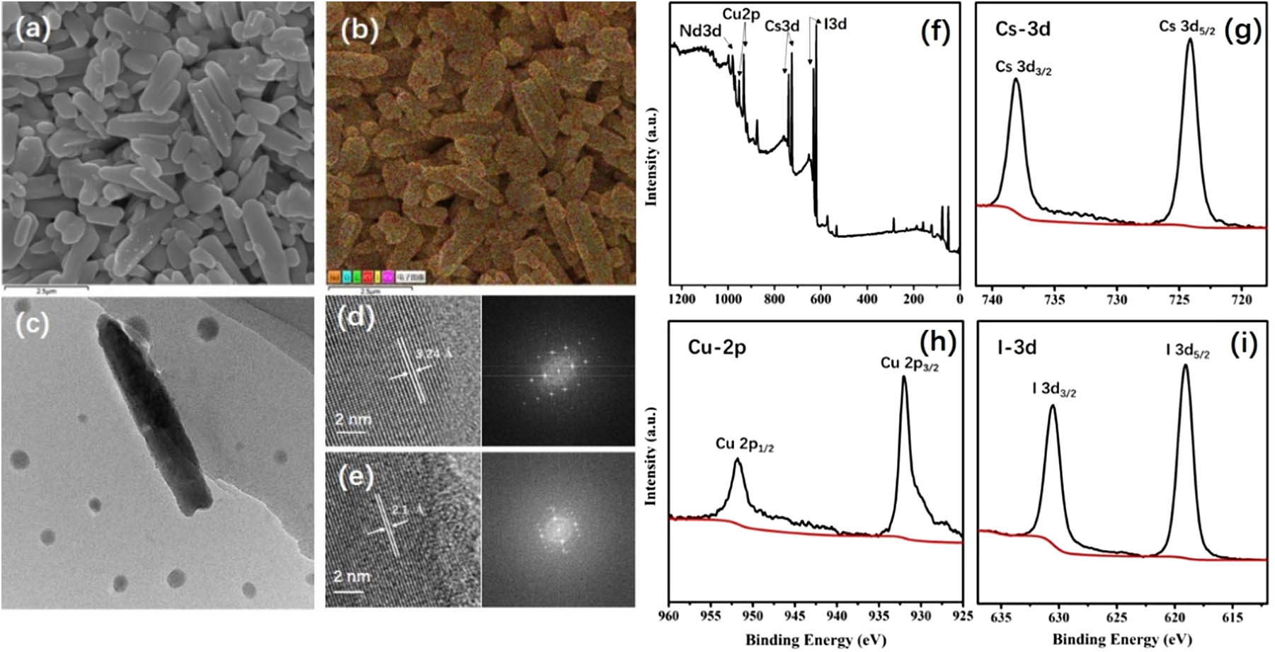
Fig. 1. (a) SEM, (b) EDS mapping, and (c) TEM images of the sample with NdI 3 Cs 3 Cu 2 I 5 CsCu 2 I 3 NdI 3 3 d 2 p 3 d
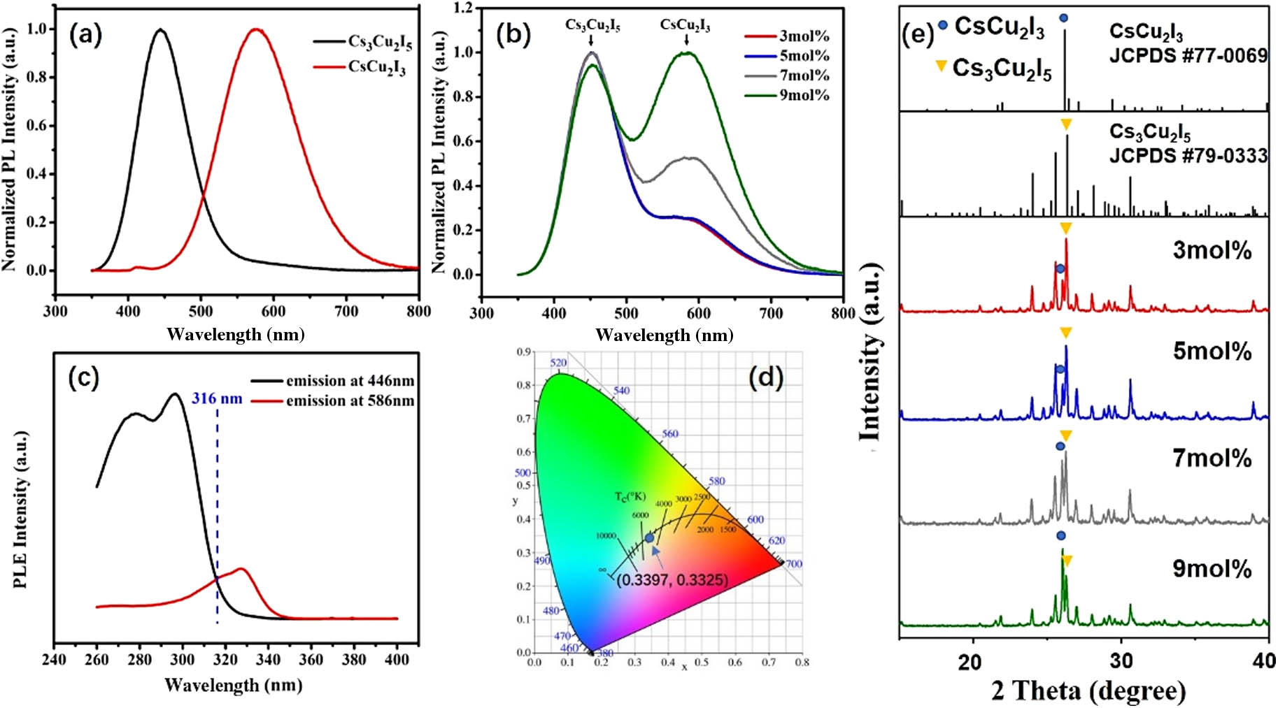
Fig. 2. (a) PL spectra of pure Cs 3 Cu 2 I 5 CsCu 2 I 3 NdI 3 Cs 3 Cu 2 I 5 CsCu 2 I 3 NdI 3 NdI 3 NdI 3 Cs 3 Cu 2 I 5 CsCu 2 I 3
Fig. 3. Crystal structures of (a) Cs 3 Cu 2 I 5 CsCu 2 I 3
Fig. 4. (a) PL spectra under excitation wavelength of 320 nm. (b) XRD patterns of the samples with NdI 3 CsCu 2 I 3
Fig. 5. (a) PL spectra of samples with 9 mol% concentration of NdI 3 TbI 3 PrI 3 BiI 3 NdI 3 TbI 3 PrI 3 NdI 3 TbI 3 PrI 3 BiI 3 NdI 3 TbI 3 NdI 3 TbI 3 PrI 3 BiI 3

Set citation alerts for the article
Please enter your email address
© Copyright 2018-2021 | Chinese Laser Press. All Rights Reserved 沪ICP备15018463号-20