• Chinese Optics Letters
  • Vol. 19, Issue 10, 103001 (2021)
Junze Li, Junchao Hu, Jiaqi Ma, Xinglin Wen, and Dehui Li*
Author Affiliations
  • School of Optical and Electronic Information and Wuhan National Laboratory for Optoelectronics, Huazhong University of Science and Technology, Wuhan 430074, China
  • show less
    DOI: 10.3788/COL202119.103001 Cite this Article Set citation alerts
    Junze Li, Junchao Hu, Jiaqi Ma, Xinglin Wen, Dehui Li. Identifying self-trapped excitons in 2D perovskites by Raman spectroscopy [Invited][J]. Chinese Optics Letters, 2021, 19(10): 103001 Copy Citation Text show less

    Abstract

    Two-dimensional (2D) perovskites exhibit broadband emission due to strong exciton–phonon coupling-induced self-trapped excitons and thus would find important applications in the field of white-light emitting devices. However, the available identifying methods for self-trapped excitons are currently rather limited and complex. Here, we identify the existence of self-trapped excitons by Raman spectroscopy in both excited and non-excited states. Under excited states, the shifting of the Raman peak indicates the presence of the lattice distortion, which together with the extra Raman scattering peak reveals the presence of self-trapped excitons. Our work provides an alternative simple method to study self-trapped excitons in 2D perovskites.

    1. Introduction

    The strong coupling between the crystal lattice and excitons would lead to the generation of self-trapped excitons (STEs)[1,2], which are one type of bound state excitons. Unlike bound state excitons usually formed by binding to defects, STE can be produced even in a perfect crystal lattice, which is created by the deformation of the crystal lattice under the coupling effect due to the softness of the crystal lattice[1,3]. Once the excitation is removed, the coupling disappears, and the lattice will return to its original state, resulting in removal of STE[4]. Therefore, STE can be regarded as one type of trapped state that exists only under an excited state[4]. STE exhibits broadband emissions with a large Stokes shift below the bandgap, which is beneficial to the white-light emitting devices[510]. Identifying and investigating the basic physical properties of STE is the basis for designing optoelectronic devices and optimizing device performance.

    Recent studies reveal that two-dimensional (2D) perovskites show strong broadband luminescence, which is attributed to STE emission[5,1114]. Usually, STEs are only present under excited states, and thus it is a great challenge to directly detect them[4]. The intensity of STE is related to the temperature, the dimension of the materials, and the exciton–phonon coupling strength[3]; however, it is still difficult to distinguish STE from defect emissions at present. Currently, two strategies are usually adopted to identify the presence of STE, which are the ultrafast spectroscopy technique[3,15,16] and the evaluation of exciton–phonon coupling strength extracted from absorption and luminescence spectra[9,10,17]. The former requires an expensive femtosecond laser, while the latter generally needs to carry out temperature-dependent measurements, and the error of experimental fitting is also unavoidable. Therefore, it is desirable to find a simple and efficient method to identify and study STE in 2D perovskites.

    Here, we report on the identification of STE in 2D perovskite crystals by Raman spectroscopy. By measuring the Raman spectra of the (C8H9NH3)2PbI4[(PEA)2PbI4] 2D perovskite under excitation of the 2.33 eV and 1.96 eV lasers, we observed red shifting of Raman peaks in the excited states, revealing lattice distortion under the excited states. In addition, the extra Raman scattering peak under the excited states further confirms the formation of STE.

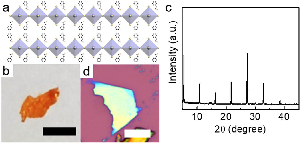
    2. Crystal Preparation

    (PEA)2PbI4 perovskite crystals are synthesized according to the previously reported solution method[1820]. The structure of (PEA)2PbI4 can be regarded as an inorganic layer of [PbI6]2 octahedral sandwiched by two layers of phenethylammonium (PEA) organic cations [Fig. 1(a)]. The color of the as-synthesized crystal is orange, which is consistent with previous reports [Fig. 1(b)][21]. A powder X-ray diffraction (XRD) pattern [Fig. 1(c)] of as-synthesized crystals shows that all diffraction peaks can be indexed to the (00l) direction, similar to previous reports[21]. The 2D perovskite flakes were exfoliated from bulk crystals and transferred onto a silicon substrate for the following optical measurements [Fig. 1(d)][22].

    (a) Schematic of (PEA)2PbI4 crystal structure. (b) Optical microscope image of the as-synthesized crystal. Scale bar: 2 mm. (c) Powder XRD pattern of as-synthesized crystals. (d) Optical microscope image of an exfoliated flake. Scale bar: 10 µm.

    Figure 1.(a) Schematic of (PEA)2PbI4 crystal structure. (b) Optical microscope image of the as-synthesized crystal. Scale bar: 2 mm. (c) Powder XRD pattern of as-synthesized crystals. (d) Optical microscope image of an exfoliated flake. Scale bar: 10 µm.

    3. Self-Trapped Exciton Emission

    Figure 2 displays the photoluminescence (PL) spectra of as-synthesized crystals at 80 K under different laser excitation. Under a 2.62 eV laser excitation, which is larger than the excitonic energy of (PEA)2PbI4 (∼2.36 eV), the crystal can be excited, and thus there are emission peaks of both free excitons (X0) and STE (XSTE)[23]. Similarly, when the excitation beam with an energy of 2.33 eV is located at the band-edge of (PEA)2PbI4, the crystal can still be excited, and only STE emission is present. The emission peak of STE excited by the 2.33 eV laser shows a blue shift compared with the spectrum excited by the 2.62 eV laser, which might be due to the heating effect. In contrast, when the energy of the excitation beam (1.96 eV) is far lower than the bandgap of 2D perovskite crystals, no emission peak can be observed except for a sharp line (PSi) close to the excitation laser, which can be ascribed to the Raman signal from the silicon substrate. Those observations clearly indicate that STE only exists in excited states, agreeing with previous reports[4].

    PL spectra of a (PEA)2PbI4 crystal under different excitation at 80 K.

    Figure 2.PL spectra of a (PEA)2PbI4 crystal under different excitation at 80 K.

    We have further carried out temperature-dependent PL studies. Figures 3 and 4 show the temperature-dependent PL spectra excited by the 2.33 eV and 1.96 eV lasers, respectively. We intentionally plot them at the same intensity scale for comparison. With the increase of temperature, the intensity of STE emission gradually decreases under the 2.33 eV laser excitation [Fig. 3(a)], while no emission peak is present for all of temperatures we investigated under a 1.96 eV excitation [Fig. 3(b)]. This further confirms that STE must be formed under excited states and independent of the surrounding temperature.

    PL spectra of a (PEA)2PbI4 crystal excited by (a) 2.33 eV and (b) 1.96 eV lasers at different temperatures.

    Figure 3.PL spectra of a (PEA)2PbI4 crystal excited by (a) 2.33 eV and (b) 1.96 eV lasers at different temperatures.

    Raman spectra of a (PEA)2PbI4 crystal under 2.33 eV (black) and 1.96 eV (red) laser excitation at 80 K. The positions of all peaks are 76 cm−1(P1), 102.5 cm−1(P2), 134 cm−1(P3) (non-excited state), and 79.6 cm−1(P1), 108.5 cm−1(P2), 134 cm−1(P3), 160.8 cm−1(P4) (excited state).

    Figure 4.Raman spectra of a (PEA)2PbI4 crystal under 2.33 eV (black) and 1.96 eV (red) laser excitation at 80 K. The positions of all peaks are 76cm1(P1), 102.5cm1(P2), 134cm1(P3) (non-excited state), and 79.6cm1(P1), 108.5cm1(P2), 134cm1(P3), 160.8cm1(P4) (excited state).

    4. Raman Spectroscopy

    We have measured the Raman spectra of (PEA)2PbI4 under both excited states and non-excited states to investigate how the STE can alter the Raman spectrum. The Raman spectra under excited states and non-excited states are collected under the 2.33 eV and 1.96 eV laser excitation, respectively. All Raman spectra were calibrated by using a silicon wafer. Figure 4 indicates that there are three peaks (labeled as P1,P2,P3) under both excited and non-excited states, whereas an additional peak appears under the excited states (labeled as P4). In order to eliminate the influence from sample degradation[24], we changed the excitation laser from 1.96 eV to 2.33 eV and back to 1.96 eV for cyclic measurement, and no apparent difference in Raman spectra can be observed, suggesting that a difference in the Raman spectra between excited and non-excited states indeed originates from the excited states. According to a previous report, we assign P1 to Pb-I bond bending and twisting, P2 to out-of-plane Pb-I bond stretching, and P3 to in-plane Pb-I bond stretching[25].

    In addition, compared with the spectrum under non-excited states, P1 and P2 show a red shift under the excited states, while P3 remains at the same position. It has been reported that the shifting of the Raman scattering peak can reflect the change of vibration mode and lattice distortion[26,27]. Therefore, the shifting of P1 and P2 indicating the bending and twisting of Pb-I bonds in the out-of-plane direction is changed. Since STE is created due to the lattice distortion caused by exciton–phonon coupling, it is reasonable to use Raman peak shifting to identify the existence of lattice distortion and further the presence of STE.

    In order to investigate the origin of P4, we have acquired Raman spectra at different temperatures. There are always three peaks under non-excited states for all temperatures that we investigated, and all peaks are not sensitive to temperature [Fig. 5(a)]. In contrast, under the excited states, the relative intensities of P1, P2, and P3 are changed against temperature, while P4 is rather sensitive to temperature and disappears above 140 K [Fig. 5(b)]. Similar to GaAs when a new Raman scattering peak from localized holes emerges at low temperature[28,29], we assign the P4 peak to the Raman signal of STEs, which are a type of localized excitons. This assignment is further supported by the correlation between the STE emission in the PL spectra and the P4 signal in Raman spectra. The STE emission is greatly enhanced below 140 K [Fig. 3(a)], and simultaneously P4 scattering peaks are present below 140 K [Fig. 5(b)].

    Temperature-dependent Raman spectra of a (PEA)2PbI4 crystal under non-excited states excited by (a) 1.96 eV and (b) 2.33 eV lasers, respectively.

    Figure 5.Temperature-dependent Raman spectra of a (PEA)2PbI4 crystal under non-excited states excited by (a) 1.96 eV and (b) 2.33 eV lasers, respectively.

    The evolution of the Raman peak position with temperature under excited states and non-excited states is also extracted from Fig. 5 and plotted in Fig. 6. All Raman peaks exhibit a red shift as the temperature increases. Nevertheless, P1 and P2 under excited states show an overall blue shift compared with that under non-excited states. Therefore, we can exclude the possibility that the observed Raman shifting under excited states is actually from the laser heating effect.

    Raman peak versus temperature extracted from Fig. 5. The gray dot lines are used to guide the eye.

    Figure 6.Raman peak versus temperature extracted from Fig. 5. The gray dot lines are used to guide the eye.

    We have also measured the Raman spectra of (PEA)2PbBr4 perovskite crystals for comparison. There is no Raman peak shifting and no additional Raman under both 2.33 eV and 1.96 eV laser excitation (Fig. 7). Since the bandgap of (PEA)2PbBr4 is 3.02 eV, both 2.33 eV and 1.96 eV lasers are unable to excite (PEA)2PbBr4. As a result, no STE can be formed under both laser excitations. Therefore, this observation further verifies that the Raman peak shifting and the presence of an extra Raman peak in (PEA)2PbI4 under excited states are due to STE.

    Raman spectra of (PEA)2PbBr4 under 2.33 eV (black) and 1.96 eV (red) laser excitation at 80 K.

    Figure 7.Raman spectra of (PEA)2PbBr4 under 2.33 eV (black) and 1.96 eV (red) laser excitation at 80 K.

    5. Conclusions

    In summary, we have investigated the Raman spectra of (PEA)2PbI4 under both excited states and non-excited states. The Raman peaks P1 and P2 show a red shift under excited states, indicating the distortion of the crystal lattice, whereas the temperature-sensitive Raman peak P4 under excited states verifies the presence of STE. Raman peak shifting and extra Raman scattering peaks can be borrowed to identify the existence of STE in 2D perovskites. Our work provides an alternative simple method to study STE in 2D perovskites and promotes more investigations on STE-based optoelectronic devices.

    References

    [1] R. T. Williams, K. S. Song. The self-trapped exciton. J. Phys. Chem. Solids, 51, 679(1990).

    [2] H. Nishimura, T. Yamaoka, K.-I. Mizuno, M. Iemura, A. Matsui. Luminescence of free and self-trapped excitons in α-and β-perylene crystals. J. Phys. Soc. Jpn., 53, 3999(1984).

    [3] X. Wu, M. T. Trinh, D. Niesner, H. Zhu, Z. Norman, J. S. Owen, O. Yaffe, B. J. Kudisch, X.-Y. Zhu. Trap states in lead iodide perovskites. J. Am. Chem. Soc., 137, 2089(2015).

    [4] S. Kahmann, E. K. Tekelenburg, H. Duim, M. E. Kamminga, M. A. Loi. Extrinsic nature of the broad photoluminescence in lead iodide-based Ruddlesden–Popper perovskites. Nat. Commun., 11, 2344(2020).

    [5] M. D. Smith, H. I. Karunadasa. White-light emission from layered halide perovskites. Acc. Chem. Res., 51, 619(2018).

    [6] S. Li, J. Luo, J. Liu, J. Tang. Self-trapped excitons in all-inorganic halide perovskites: fundamentals, status, and potential applications. J. Phys. Chem. Lett., 10, 1999(2019).

    [7] J. Li, H. Wang, D. Li. Self-trapped excitons in two-dimensional perovskites. Front. Optoelectron., 13, 225(2020).

    [8] Q. Zhang, Y. Ji, Z. Chen, D. Vella, X. Wang, Q. H. Xu, Y. Li, G. Eda. Controlled aqueous synthesis of 2D hybrid perovskites with bright room-temperature long-lived luminescence. J. Phys. Chem. Lett., 10, 2869(2019).

    [9] M. Cong, B. Yang, F. Hong, T. Zheng, Y. Sang, J. Guo, S. Yang, K. Han. Self-trapped exciton engineering for white-light emission in colloidal lead-free double perovskite nanocrystals. Sci. Bull., 65, 1078(2020).

    [10] J. Luo, X. Wang, S. Li, J. Liu, Y. Guo, G. Niu, L. Yao, Y. Fu, L. Gao, Q. Dong, C. Zhao, M. Leng, F. Ma, W. Liang, L. Wang, S. Jin, J. Han, L. Zhang, J. Etheridge, J. Wang, Y. Yan, E. H. Sargent, J. Tang. Efficient and stable emission of warm-white light from lead-free halide double perovskites. Nature, 563, 541(2018).

    [11] L. Mao, Y. Wu, C. C. Stoumpos, M. R. Wasielewski, M. G. Kanatzidis. White-light emission and structural distortion in new corrugated two-dimensional lead bromide perovskites. J. Am. Chem. Soc., 139, 5210(2017).

    [12] E. R. Dohner, A. Jaffe, L. R. Bradshaw, H. I. Karunadasa. Intrinsic white-light emission from layered hybrid perovskites. J. Am. Chem. Soc., 136, 13154(2014).

    [13] M. D. Smith, B. A. Connor, H. I. Karunadasa. Tuning the luminescence of layered halide perovskites. Chem. Rev., 119, 3104(2019).

    [14] S. Zhang, Y. Zhong, F. Yang, Q. Cao, W. Du, J. Shi, X. Liu. Cavity engineering of two-dimensional perovskites and inherent light-matter interaction. Photon. Res., 8, A72(2020).

    [15] T. Hu, M. D. Smith, E. R. Dohner, M.-J. Sher, X. Wu, M. T. Trinh, A. Fisher, J. Corbett, X.-Y. Zhu, H. I. Karunadasa, A. M. Lindenberg. Mechanism for broadband white-light emission from two-dimensional (110) hybrid perovskites. J. Phys. Chem. Lett., 7, 2258(2016).

    [16] A. Yangui, D. Garrot, J. S. Lauret, A. Lusson, G. Bouchez, E. Deleporte, S. Pillet, E. E. Bendeif, M. Castro, S. Triki, Y. Abid, K. Boukheddaden. Optical investigation of broadband white-light emission in self-assembled organic-inorganic perovskite (C6H11NH3)2PbBr4. J. Phys. Chem. C, 119, 23638(2015).

    [17] J. Li, J. Wang, J. Ma, H. Shen, L. Li, X. Duan, D. Li. Self-trapped state enabled filterless narrowband photodetections in 2D layered perovskite single crystals. Nat. Commun., 10, 806(2019).

    [18] J. Wang, J. Li, Q. Tan, L. Li, J. Zhang, J. Zang, P. Tan, J. Zhang, D. Li. Controllable synthesis of two-dimensional Ruddlesden–Popper-type perovskite heterostructures. J. Phys. Chem. Lett., 8, 6211(2017).

    [19] Y. Q. Zhao, Q. R. Ma, B. Liu, Z. L. Yu, J. Yang, M. Q. Cai. Layer-dependent transport and optoelectronic property in two-dimensional perovskite: (PEA)2PbI4. Nanoscale, 10, 8677(2018).

    [20] Y.-T. Li, L. Ding, J.-Z. Li, J. Kang, D.-H. Li, L. Ren, Z.-Y. Ju, M.-X. Sun, J.-Q. Ma, Y. Tian, G.-Y. Gou, D. Xie, H. Tian, Y. Yang, L.-W. Wang, L.-M. Peng, T.-L. Ren. Light-enhanced ion migration in two-dimensional perovskite single crystals revealed in carbon nanotubes/two-dimensional perovskite heterostructure and its photomemory application. ACS Cent. Sci., 5, 1857(2019).

    [21] Y. Liu, H. Ye, Y. Zhang, K. Zhao, Z. Yang, Y. Yuan, H. Wu, G. Zhao, Z. Yang, J. Tang, Z. Xu, S. Liu. Surface-tension-controlled crystallization for high-quality 2D perovskite single crystals for ultrahigh photodetection. Matter, 1, 465(2019).

    [22] J. Li, J. Wang, Y. Zhang, H. Wang, G. Lin, X. Xiong, W. Zhou, H. Luo, D. Li. Fabrication of single phase 2D homologous perovskite microplates by mechanical exfoliation. 2D Mater., 5, 021001(2018).

    [23] D. B. Straus, S. Hurtado Parra, N. Iotov, J. Gebhardt, A. M. Rappe, J. E. Subotnik, J. M. Kikkawa, C. R. Kagan. Direct observation of electron-phonon coupling and slow vibrational relaxation in organic-inorganic hybrid perovskites. J. Am. Chem. Soc., 138, 13798(2016).

    [24] Z. Dang, Y. Luo, X.-S. Wang, M. Imran, P. Gao. Electron-beam-induced degradation of halide-perovskite-related semiconductor nanomaterials. Chin. Opt. Lett., 19, 030002(2021).

    [25] B. Dhanabalan, Y. C. Leng, G. Biffi, M. L. Lin, P. H. Tan, I. Infante, L. Manna, M. P. Arciniegas, R. Krahne. Directional anisotropy of the vibrational modes in 2D-layered perovskites. ACS Nano, 14, 4689(2020).

    [26] B. Robert. Resonance Raman spectroscopy. Photosynth. Res., 101, 147(2009).

    [27] H. Hashimoto, Y. Koyama. Raman spectra of all-trans-β-carotene in the S1 and T1 states produced by direct photoexcitation. Chem. Phys. Lett., 163, 251(1989).

    [28] X. Shen. Semiconductor Spectrum and Optical Properties,, 553(2002).

    [29] P. Verma, S. C. Abbi, K. P. Jain. Raman-scattering probe of anharmonic effects in GaAs. Phys. Rev. B, 51, 16660(1995).

    Junze Li, Junchao Hu, Jiaqi Ma, Xinglin Wen, Dehui Li. Identifying self-trapped excitons in 2D perovskites by Raman spectroscopy [Invited][J]. Chinese Optics Letters, 2021, 19(10): 103001
    Download Citation