Abstract
The all-optical approach plays an important role in ultrafast all-optical signal processing, and the all-fiber scheme has a wide application in optical communications. In this letter, we investigate an all-optical modulator using few-layer molybdenum disulfide ()-polyvinyl alcohol (PVA) thin films based on the thermo-optic effect and obtain a long-time stable modulated output by applying polarization interference. By absorbing the injected 980 nm pump (control light), generates heat, changes the refractive index of , and modulates the polarization of light. The obtained thermal all-optical modulator has a rise time of 526 μs.Since the discovery of graphene in 2004, two-dimensional (2D) materials have attracted widespread attention[1–3]. Many researchers have investigated novel optoelectronic devices based on graphene, including optical modulators[4,5], switches[6], and polarizers[7]. In recent years, other kinds of 2D materials, including transition metal dichalcogenides (TMDs), topological insulators (TIs)[8,9], and black phosphorus (BP)[10–12] have also been investigated. In particular, TMDs have become a research hotspot due to their similar photonic and electronic properties[13–15], including high optical nonlinearity[16] and saturable absorption[17,18]. Many researchers have demonstrated the applications of these TMDs as saturable absorbers in Q-switched fiber lasers and mode-locked fiber lasers[17,19].
Meanwhile, the all-optical scheme plays an important role in optical communications, including all-optical modulation, routing, and sensing. There have been some demonstrations of all-optical modulators and phase shifters based on graphene[4–6]. Recently, an all-optical phase shifter near 1550 nm using few-layer 2D material tungsten disulfide () deposited on a tapered fiber has been reported[20]. Wu et al. demonstrate an all-optical switch by embedding the phase shifter into one arm of a fiber Mach–Zehnder interferometer (MZI) with good control efficiency and high extinction ratio. However, the fiber MZI structure makes the device sensitive to the environmental perturbation.
In this work, we demonstrate a fiber all-optical modulator using few-layer molybdenum disulfide ()-polyvinyl alcohol (PVA) thin films. The device is based on polarization interference in an optical fiber, and the thermo-optic effect of -PVA thin film is utilized as a control mechanism. By absorbing the pump at 980 nm, generates heat, changes the refractive index of the -PVA thin film, and modifies the polarization of the incident light at 1550 nm. The demonstrated all-optical modulator has a rise time of 526 μs. Since all the control and signal beams propagate in the same fiber, the environmental perturbation, e.g., air flow and temperature change, induces common mode disturbance and has very weak influence on the device operation. Thus, our device is less sensitive to the environmental perturbation compared to the MZI structure. The filmy also provides advantages in the practical applications due to its compactness. The device based on -PVA thin film proves the potential of 2D TMDs for all-optical signal processing devices.
Sign up for Chinese Optics Letters TOC. Get the latest issue of Chinese Optics Letters delivered right to you!Sign up now
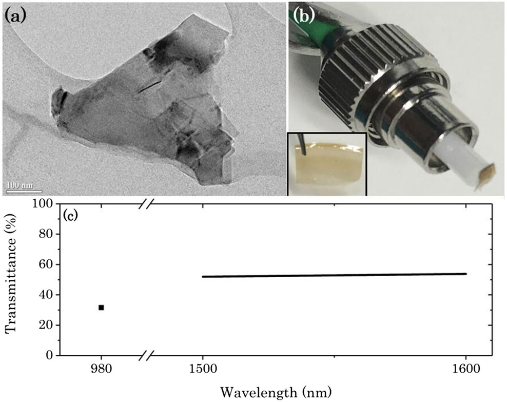
A high-quality -PVA thin film is the key component in the all-optical modulator, which provides significant flexibility in practical applications. By using the liquid-phase exfoliation (LPE) method[19], -PVA water dispersions with sodium cholate (SC, as a surfactant) are prepared. The detailed preparation of dispersions can be referred to Ref. [19]. The transmission electron microscope (TEM) image of nanosheets is shown in Fig. 1(a). nanosheets with the size of a few hundreds of nanometers can be observed. Then, 2 mL -PVA dispersions are mixed with 10 mL PVA solution for 24 h by using a magnetic stirrer. The mixture is processed with an ultrasonic water bath for another 4 h. Then, the -PVA mixture is transferred to the surface of a clean plastic dish and dried under a 50°C condition for three days to form a thin film. The -PVA thin film is further cut into small pieces and transferred onto the end facet of an optical fiber connector for experimental usage, as shown in Fig. 1(b); the inset is the fabricated -PVA thin film. The prepared -PVA thin film is sandwiched between two fiber-optic connectors/angled physical contact (FC/APC) fiber connectors. Figure 1(c) shows the measured transmission spectrum of the -PVA thin film. The insertion loss of the -PVA thin film is at 980 nm and near 1550 nm.

Figure 1.(a) TEM image of nanosheets in the dispersions, (b) -PVA film transferred onto a fiber end, inset: -PVA thin film, and (c) transmission spectrum of -PVA thin film.
Figure 2 shows the experimental setup of an all-optical modulator with the -PVA thin film. The 980 nm pump light (control light) is generated by injecting a square-wave electronic signal into the analog modulation port of the pump driver. The signal light is generated by a 1550 nm continuous wave (CW) laser source. Control and signal light beams are combined through a wavelength division multiplexer (WDM). The polarizations of two light beams are controlled by the polarization controllers (PCs) for a more stable output signal. The -PVA thin film is sandwiched between two FC/APC fiber connectors after the WDM. A second WDM after the -PVA thin film is used to filter out the residual 980 nm pump light. A polarizer after the second WDM selects the desired polarization state of the signal light and generates modulation outputs. The input signal light at 1550 nm is the CW light. When the 980 nm pulsed pump light is injected, the output of the device is 1550 nm of pulsed light controlled by the 980 nm pump light, and the output is 1550 nm of CW light without the input of the 980 nm pulsed pump light. The output signal is then characterized by a 2.5 GHz oscilloscope (Agilent DSO9254 A) with a photodetector for its time-domain properties.
Figure 2.Experimental setup of an all-optical modulator with -PVA thin film.
Figure 3 summarizes the output properties of the modulated pulses. When the 980 nm pump light is injected, absorbs the pump light, generates heat, changes the refractive index of the -PVA thin film due to the thermo-optic effect, and modifies the polarization of the signal light. The transmission loss of the 980 nm pump from the PC and the first WDM to the second WDM is with 4 dB of loss due to PC and two WDMs and 5 dB of absorption from the . The applied square-wave pump light has a repetition rate of 50 Hz, a pulse width of 4 ms, and a duty cycle of 20%. The average power of the 980 pump light before is . Figure 3(a) shows the measured waveforms of the pump power (inset) and the modulated output signal. A bright on–off operation of the device can be observed. We can also find that both the rising edge and the falling edge of the modulated output have been flattened due to the bandwidth limitation of the thermo-optic effect. Figure 3(b) shows an enlarged view of a single output pulse. The rise time is 526 μs, which is obtained by calculating the rise time of the signal power from 10% to 90%. By fitting the waveform with exponential decay functions of for the rising edge and for the falling edge, the time constants are estimated to be and , shown as the red curve in Fig. 3(b). The time constant for the rising edge is determined by the heating process that the absorbs pump light to raise the temperature and the heat dissipation to the substrate. The time constant for the falling edge is only related to the heat dissipation of the -PVA thin film because there is no longer pump light. The long-time stability of the output is also investigated, as shown in Fig. 3(c). It can be observed that a long stable pulse train can be obtained, which shows that the method of the polarized interference is less sensitive to the environmental disturbance compared to the MZI structure reported in our previous work[20].
Figure 3.(a) Modulated output signal, inset: pulsed pump light, (b) a zoomed view of a single off-on-off transition of the output pulse (black) and exponential fit (red), and (c) a long-time stable output.
The switching time is an important parameter for an all-optical modulator. The rising edge of the output pulse is determined by the heating process from the pump pulse and heat dissipation to the air, while the falling edge is only due to the heat dissipation. To investigate it, pump pulses with fixed peak power and different duty cycles are adopted. The corresponding output pulses are shown in Fig. 4(a). It can be found that the output pulses are generated by the pump pulses with different duty cycles, but the same peak power results in the same rise time. That is, with the same peak power of the pump pulses, the instant heat generation is unchanged. Furthermore, pump pulses with different peak powers and the same pulse energy are applied. Figure 4(b) shows the results of the output pulses with different duty cycles of the pump pulses. The duty cycle of the pulse is changed from 10% to 50%. The corresponding peak power of the pump pulse is inversely proportional to the duty cycle. The fitted time constants based on the measurement results are summarized in Table 1. It can be clearly found that the output pulses generated by the pump pulses with a lower duty cycle (and thus a higher peak power) have a shorter rise time. However, the fall time is almost constant.
| Duty Cycle (%) | Peak Pump Power (mW) | Time Constant of Rising Edge (μs) | Time Constant of Falling Edge (μs) |
|---|
| 10 | 1600 | 252.3 | 348.6 |
| 20 | 800 | 324.5 | 353.1 |
| 30 | 533 | 434.7 | 379.2 |
| 40 | 400 | 556.7 | 390.1 |
| 50 | 320 | 573.6 | 405.0 |
Table 1. Comparison of Modulated Output Pulses Generated by the Pump Pulses with Different Duty Cycles
Figure 4.Output signal pulses when the pump pulses with different duty cycles and (a) the same peak power and (b) different peak powers are applied.
To further investigate the response property of the device, a burst of three pump pulses is applied. The burst period is 1.8 ms, and, in each burst, the pulses have a period of 200 μs (5 kHz repetition rate) and a duty cycle of 90%, as shown in Fig. 5(a). When the burst signal is injected, the output signal is shown as Fig. 5(b). It can be observed that the output signal exhibits the property similar to the charge–discharge process of a capacitor. This result demonstrates the accumulation property of the device, which is clear proof of the thermal effect.
Figure 5.(a) Burst of pulsed pump light and (b) device output.
In conclusion, a proof-of-concept all-optical modulator has been demonstrated by using -PVA thin film based on the thermo-optic effect. By adopting the method of the polarization interference, an optical modulator is obtained with a rise time of 526 μs, and the time constant of the rising edge is . The scheme is less sensitive to the environmental perturbation compared to the MZI structure, thus, a long-time stable pulse train is obtained. Moreover, the with a thin-film form provides significant flexibility in the practical applications because of its compactness. Our work may pave the way for exploring TMD materials for more potential in all-optical signal processing, such as optical logic gate, routing, and sensing.
References
[1] F. Bonaccorso, Z. Sun, T. Hasan, A. C. Ferrari. Nat. Photon., 4, 611(2010).
[2] A. Martinez, K. Fuse, B. Xu, S. Yamashita. Opt. Express, 18, 23054(2010).
[3] N. Papasimakis, Z. Luo, Z. X. Shen, F. De Angelis, E. Di Fabrizio, A. E. Nikolaenko, N. I. Zheludev. Opt. Express, 18, 8353(2010).
[4] W. Li, B. Chen, C. Meng, W. Fang, Y. Xiao, X. Li, Z. Hu, Y. Xu, L. Tong, H. Wang, W. Liu, J. Bao, Y. R. Shen. Nano Lett., 14, 955(2014).
[5] S. Yu, X. Wu, K. Chen, B. Chen, X. Guo, D. Dai, L. Tong, W. Liu, Y. R. Shen. Optica, 3, 541(2016).
[6] X. Gan, C. Zhao, Y. Wang, D. Mao, L. Fang, L. Han, J. Zhao. Optica, 2, 468(2015).
[7] Q. Bao, H. Zhang, B. Wang, Z. Ni, C. H. Y. X. Lim, Y. Wang, D. Y. Tang, K. P. Loh. Nat. Photon., 5, 411(2011).
[8] J. Lee, J. Koo, Y. M. Jhon, J. H. Lee. Opt. Express, 22, 6165(2014).
[9] Z. Luo, M. Liu, H. Liu, X. Zheng, A. Luo, C. Zhao, H. Zhang, S. Wen, W. Xu. Opt. Letters, 38, 5212(2013).
[10] Z. Luo, M. Liu, Z. Guo, X. Jiang, A. Luo, C. Zhao, X. Yu, W. Xu, H. Zhang. Opt. Express, 23, 20030(2015).
[11] X. Ren, Z. Li, Z. Huang, D. Sang, H. Qiao, X. Qi, J. Li, J. Zhong, H. Zhang. Adv. Funct. Mater., 27, 1606834(2017).
[12] L. Kong, Z. Qin, G. Xie, Z. Guo, H. Zhang, P. Yuan, L. Qian. Laser Phys. Lett., 13, 045801(2016).
[13] K. Wang, J. Wang, J. Fan, M. Lotya, A. O’Neill, D. Fox, Y. Feng, X. Zhang, B. Jiang, Q. Zhao, H. Zhang, J. N. Coleman, L. Zhang, W. J. Blau. ACS Nano, 7, 9260(2013).
[14] R. I. Woodward, R. C. T. Howe, G. Hu, F. Torrisi, M. Zhang, T. Hasan, E. J. R. Kelleher. Photon. Res., 3, A30(2015).
[15] X. Zhang, S. Zhang, C. Chang, Y. Feng, Y. Li, N. Dong, K. Wang, L. Zhang, W. J. Blau, J. Wang. Nanoscale, 7, 2978(2015).
[16] K. Wang, Y. Feng, C. Chang, J. Zhan, C. Wang, Q. Zhao, J. N. Coleman, L. Zhang, W. J. Blau, J. Wang. Nanoscale, 6, 10530(2014).
[17] B. Chen, X. Zhang, K. Wu, H. Wang, J. Wang, J. Chen. Opt. Express, 23, 26723(2015).
[18] C. Guo, B. Chen, H. Wang, X. Zhang, J. Wang, K. Wu, J. Chen. IEEE Photon. J., 8, 1(2016).
[19] K. Wu, X. Zhang, J. Wang, X. Li, J. Chen. Opt. Express, 23, 11453(2015).
[20] K. Wu, C. Guo, H. Wang, X. Zhang, J. Wang, J. Chen. Opt. Express, 25, 17639(2017).