
Sunae So, Younghwan Yang, Taejun Lee, Junsuk Rho. On-demand design of spectrally sensitive multiband absorbers using an artificial neural network[J]. Photonics Research, 2021, 9(4): B153
- Photonics Research
- Vol. 9, Issue 4, B153 (2021)
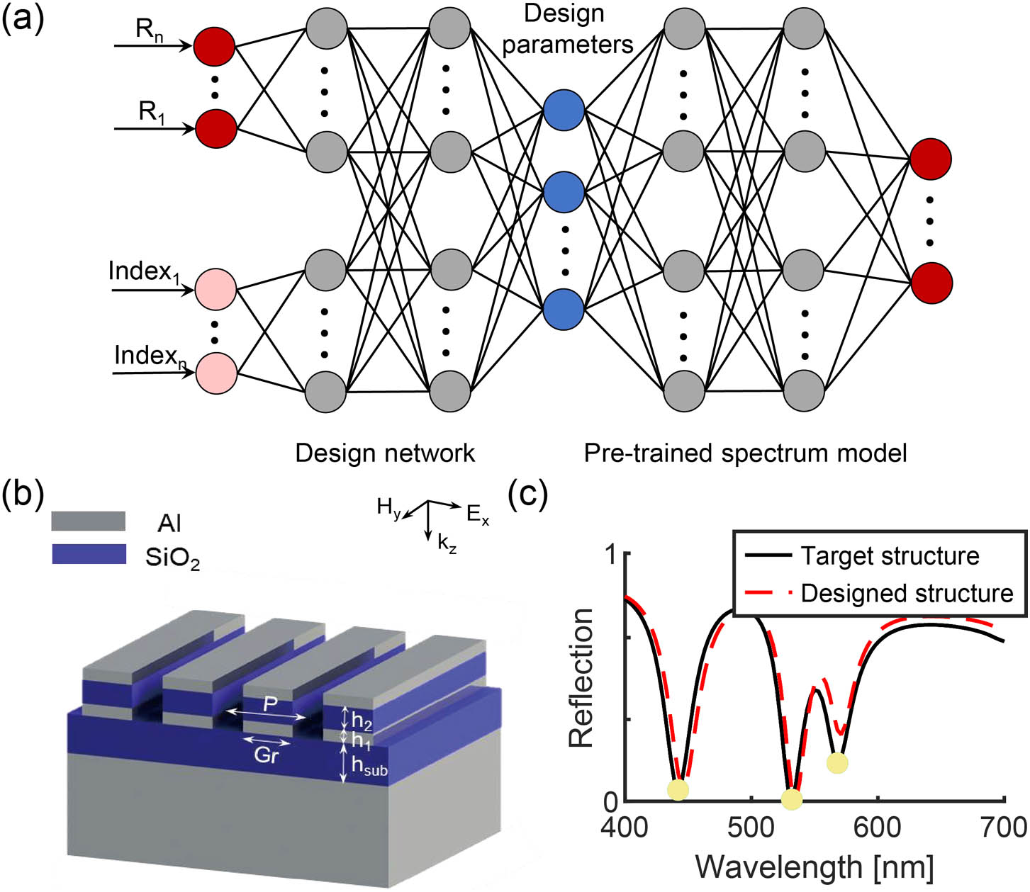
Fig. 1. Schematic of the designing grating structures for multiband absorbers. (a) A schematic of ANN for designing grating structures. The network is composed of two artificial neural networks of design network and pre-trained spectrum network. The design network both takes the input reflection spectra and resonant wavelengths, and the pre-trained spectrum network takes design parameters to evaluate the optical reflection spectra of the designed structures. (b) A schematic and (c) an example of optical property of a perfect multiband absorber under investigation. Yellow markers indicate resonant wavelengths.
![(a) Scanning electron microscope image of a designed grating structure with a scale bar of 1 μm. (b) Target reflection spectrum (black solid line) and designed optical properties obtained from the FDTD simulation (red dotted line) and experiment (yellow dotted line). Grating parameters with [P, Gr, h1, h2, hsub] = [245 nm, 120 nm, 42 nm, 113 nm, 195 nm] are designed by the network. (c) Examples of test results are shown. Black solid lines and red dotted lines are the input and target reflection spectra, respectively, and yellow markers are indexed resonant wavelengths.](/richHtml/prj/2021/9/4/0400B153/img_002.jpg)
Fig. 2. (a) Scanning electron microscope image of a designed grating structure with a scale bar of 1 μm. (b) Target reflection spectrum (black solid line) and designed optical properties obtained from the FDTD simulation (red dotted line) and experiment (yellow dotted line). Grating parameters with [P , Gr , h 1, h 2, h sub
Fig. 3. (a) Target (black solid line) and designed reflection spectrum. Magnetic field distribution (color maps) and electric displacement (arrow surfaces) at the resonant wavelengths of (b) 450 nm, (c) 525 nm, and (d) 600 nm.
Fig. 4. Design of multiband absorbers with (a) single, (b) double, and (c) triple resonances. The first column shows the target input spectra, and the second column shows the designed responses. The red lines indicate target resonant wavelengths. The third column shows the histogram of the MSE for a total of 51 input spectra. The insets show the average MSE of the test input.
Fig. 5. Comparison between two networks fed with and without spectral resonant wavelengths. The left is the target input spectra; the middle and the right are the predicted response of the networks without and with spectral information, respectively. The red lines are target resonant wavelengths.
Fig. 6. Analysis on output parameters for gradually changing target resonant wavelengths. (a) Target spectra with gradually changing resonant target wavelengths and (b) corresponding designed responses. For given varying input spectra, the designed parameters of (c) grating height and substrate height and (d) period and grating width.
Fig. 7. Network pruning results. Visualization of the trained weights in (a) the original network and (b) the pruned network. For each layer (L n , n = 1 , 2 , … , 7
Fig. 8. Design of multiband absorbers with (a) single, (b) double, and (c) triple resonances using the reduced network. The first column shows target input spectra, and the second column shows the designed response. The red lines indicate target resonant wavelengths. The third column shows the histogram of the MSE for a total of 51 input spectra.
|
Table 1. Hyperparameters Used in the Training of Two Networks
|
Table 2. Number of Neurons in Each Layer

Set citation alerts for the article
Please enter your email address
© Copyright 2018-2021 | Chinese Laser Press. All Rights Reserved 沪ICP备15018463号-20