Abstract
A polarization-diversity loop with a silicon waveguide with a lateral p-i-n diode as a nonlinear medium is used to realize polarization insensitive four-wave mixing. Wavelength conversion of seven dual-polarization 16-quadrature amplitude modulation (QAM) signals at 16 GBd is demonstrated with an optical signal-to-noise ratio penalty below 0.7 dB. High-quality converted signals are generated thanks to the low polarization dependence (≤0.5 dB) and the high conversion efficiency (CE) achievable. The strong Kerr nonlinearity in silicon and the decrease of detrimental free-carrier absorption due to the reverse-biased p-i-n diode are key in ensuring the high CE levels.1. INTRODUCTION
The stable growth of data traffic in current optical networks is pushing the need to provide higher throughput at a reduced cost per bit. All-optical signal processing (OSP) is a promising direction to achieve simultaneous processing of signals over a large optical bandwidth, thus potentially reducing the overall cost [1,2]. Among the several promising OSP functionalities that have been proposed, optical wavelength conversion is particularly interesting, both to improve network usability and to implement more complex operations [3]. The possibility to resolve wavelength contentions within a network without converting signals back to the electrical domain could significantly decrease the blocking probability as well as enable the processing of multiple wavelength-division multiplexed (WDM) channels simultaneously [3]. A favorable scaling in terms of cost and energy consumption may therefore be achievable [1]. Furthermore, several more advanced processing operations can be implemented starting from a basic wavelength converter. The phase-sensitive properties of four-wave mixing (FWM)-based wavelength conversion enables low-noise amplification [4,5], signal regeneration [6–8], and advanced optical filtering [9]. Furthermore, FWM in one of its simplest configurations results in phase conjugation of the generated idler. Such an interesting property finds applications ranging from dispersion to nonlinearity compensation and signal regeneration [10].
The potential advantages from all-optical wavelength converters have led to a strong research effort focused on nonlinear materials in order to evaluate which material platform may provide the most efficient wavelength converter. Currently, most of the demonstrations focusing on wavelength conversion in a state-of-the-art system scenario are based on highly nonlinear fibers (HNLFs) [10] or use cascaded second-order nonlinearity in periodically poled lithium niobate (PPLN) waveguides [5,11]. Whereas these media enable the processing of wavelength- and polarization-division multiplexed (PDM) signals currently deployed in coherent transmission systems, i.e., using quadrature amplitude modulation (QAM) signaling, the limited potential for integration has pushed the search towards materials based on silicon compounds which are more suited for photonics integration.
Promising results have been shown in crystalline [12,13] and amorphous silicon [14] as well as silicon-germanium [14], silicon nitride [15], AlGaAs-on-insulator [16], high-index doped glass [17], chalcogenide glass [18], and silicon–organic hybrids [19]. Among these, crystalline silicon is particularly promising as it benefits the most from the existing CMOS foundry fabrication of electronic circuits and can be easily integrated with high-speed electronics. A main challenge of using crystalline silicon for nonlinear application is caused by its material bandgap, which results in strong two-photon absorption (TPA) at telecom wavelengths (around 1550 nm) leading to free-carrier absorption (FCA). FCA depletes the pump power, thus strongly hindering the Kerr nonlinear interaction. To effectively reduce FCA and thus enable more efficient FWM, the use of a reverse-biased p-i-n diode fabricated across the silicon waveguide has been demonstrated [8,12,20–22], leading to a record-high output conversion efficiency (CE) of [20].
Sign up for Photonics Research TOC. Get the latest issue of Photonics Research delivered right to you!Sign up now
Even though the above-mentioned results are fundamental in paving the way toward practical wavelength converters, the polarization sensitivity of the devices limited most of the reported demonstrations to single-polarization applications. Being able to provide transparent processing of both polarizations of PDM signals is fundamental for applying wavelength conversion to existing optical systems. Along this direction, in Refs. [23,24], dual-polarization wavelength conversion has been demonstrated by using single-pump FWM with the pump polarization angled to balance the CE in TE and TM waveguide modes. While successful, this approach requires careful design of the waveguide to match dispersion and nonlinear properties of the waveguide such that the two orthogonal modes are not severely limited by the mode with the lowest CE. Alternatively, in Ref. [13], an on-chip polarization splitter and rotator was used to separate the two signal polarizations, process them independently in two silicon waveguides, and then recombine them in a polarization combiner. This approach relaxes the complexity in terms of dispersion engineering of the waveguide but requires additional components to be designed and fabricated.
In this work, we follow a different approach and demonstrate dual-polarization wavelength conversion in a single silicon waveguide optimized for single-polarization operation by employing an off-chip polarization diversity loop [25–29]. This strategy enables using waveguides optimized for single-polarization operation to perform dual-polarization processing. The processing of each original signal polarization takes place on the same waveguide mode (polarization) but along counterpropagating directions [26–29]. This lifts the requirements of having similar dispersion and nonlinear property of two orthogonal waveguide modes. Additionally, the use of a reverse-biased lateral p-i-n diode on the waveguide enables an increase in the achievable CE and enables the conversion of seven WDM channels carrying PDM 16-QAM at 16 GBd for an aggregate rate of 896 Gb/s.
The paper is structured as follows. In Section 2, the device fabrication is introduced. In Section 3, the polarization-insensitive FWM scheme is discussed, underlining the key challenges and proposed solutions. Section 4 presents the experimental setup used for the system demonstration, with the results reported in Section 5. Finally, Section 6 summarizes the key results.
2. DEVICE FABRICATION
The silicon waveguides have been fabricated in the SiGe-BiCMOS pilot line of IHP, and a sketch of the waveguide structure is shown in Fig. 1(a). The waveguides are manufactured on a 200 mm silicon-on-insulator (SOI) wafer with an top silicon layer and a 2 μm buffer oxide layer. The SOI wafer is patterned using deep-ultraviolet (DUV) lithography and etched to provide nano-rib waveguides with a width of and a slab thickness of . The waveguide has a lateral p-i-n diode with a separation of the p- and n- regions of , which, when reverse biased, significantly decreases the impact of FCA by effectively removing TPA-generated free carriers from the waveguide region [20]. The waveguide is 4 cm long and the total linear insertion loss (IL) of the structure (fiber-to-fiber) is 12.4 dB for 30 V reverse bias applied to the diode. The main contribution to the IL is due to the vertical grating couplers, accounting for 4.2 dB/coupler on average. The grating couplers are polarization sensitive and have been designed for TE mode operation. The linear propagation loss can then be estimated to approximately 1 dB/cm.
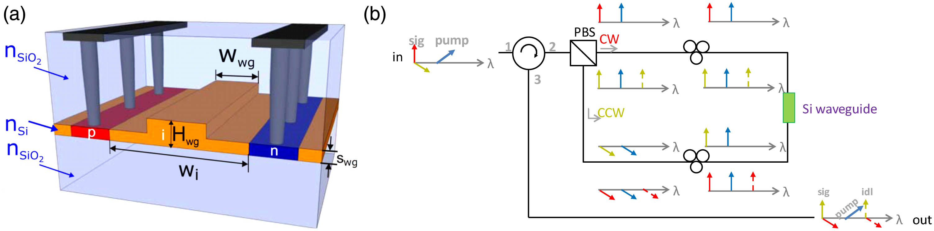
Figure 1.Sketches of (a) the silicon waveguide structure (, , and ) including the p-i-n lateral diode () and metal contacts and (b) the polarization-diversity loop setup based on the silicon waveguide highlighting CW (red arrows) and CCW (dark yellow arrows) propagation for signal (solid) and idler (dashed).
Results on devices with a similar cross section have already been reported in Refs. [8,20]. In Refs. [8,20], the slab height was 50 nm. The higher slab (100 nm) used in this work had the potential to improve the p-i-n diode efficiency [30] as well as relax the fabrication tolerances. Comparing the results reported here with Ref. [20], no relevant changes in achievable performance can be seen. The difference in slab height thus has a negligible impact.
3. POLARIZATION INSENSITIVE FOUR-WAVE MIXING
The polarization-insensitive setup demonstrated here is based on a standard-polarization diversity loop as commonly used when HNLFs are considered as the nonlinear medium of choice [25–29]. Given the polarization dependence of the input grating couplers, the loop configuration is equivalent to the case of a polarization-diversity scheme based on a polarization-maintaining HNLF (PM-HNLF) [26–29].
The scheme is shown in Fig. 1(b). A dual-polarization signal is injected into a polarization beam splitter (PBS) through a circulator (port 1 to port 2). The PBS splits two orthogonal signal polarizations into clockwise (CW) and counter-clockwise (CCW) propagation directions. Polarization controllers (PCs) within the diversity loop are used to align both CW- and CCW-propagating waves to the TE mode of the waveguide and thus automatically ensure that CW and CCW waves, after going through the waveguide, are recombined at the PBS and collected at port 3 of the circulator [Fig. 1(b)]. If a linearly polarized pump is coupled together with the dual-polarization signal with its state of polarization aligned at 45°, then the pump power gets split equally between the CW and CCW directions, and two counterpropagating co-polarized FWM processes take place in the silicon waveguide.
The conversion bandwidth of the system outlined in Fig. 1(b) is measured with the setup shown in Fig. 2. Polarization-sensitive and -insensitive scenarios are compared.

Figure 2.Experimental setup for conversion bandwidth measurements using the polarization-insensitive wavelength converter.
A weak continuous-wave signal from an external cavity laser (ECL) is polarization scrambled and coupled together with a strong continuous-wave pump generated by amplifying a second ECL in a high-power erbium-doped fiber amplifier (EDFA). Before combining signal and pump, out-of-band amplified spontaneous emission (ASE) noise from the pump EDFA is suppressed with a narrowband (0.8 nm full width at half-maximum) optical bandpass filter (OBPF). The two waves propagate through the circulator and enter the diversity loop of Fig. 1(b) through the PBS. After propagation through the loop, an optical spectrum analyzer (OSA) is used to record the optical spectra at port 3 of the circulator. From the optical spectra, the output CE, here defined as the power ratio between idler and signal at the output of the converter, is measured. The input-to-output conversion efficiency, for example defined between ports 1 and 3 of the circulator, can be calculated from the output CE by taking into account the IL of the waveguide (here 12.4 dB) and the loss of the remaining optical components in the path (in our specific implementation, approximately 2.5 dB).
Note that, whereas a silicon-waveguide-based polarization-diversity loop does not suffer from enhanced stimulated Brillouin scattering as do HNLF-based loops [28], care is required to minimize reflections at the fiber–chip interface. Using a polarization-diversity loop results in the reflection from the CW (CCW) waves at the input of the waveguide interfering with the CCW (CW) waves at the output of the waveguide. The impact of reflections rises mainly from the use of flat cleaved fibers, which result in approximately of return loss. The use of index-matching oil at the fiber–chip interface enabled bringing the return loss down to less than , which was sufficient to ensure negligible interference. Additionally, the index-matching oil provided approximately 0.5 dB decrease in coupling loss (already included in the 12.4 dB of IL mentioned above).
The conversion bandwidth has been measured by varying the signal wavelength for a fixed pump wavelength of 1545.5 nm. To test the polarization dependence of the scheme, three measurement conditions have been considered: both signal and pump aligned to the CW propagation direction and the polarization scrambler switched off (CW case), both signal and pump aligned to the CCW propagation direction and the polarization scrambler switched off (CCW case), and signal polarization scrambled and pump polarization aligned such that the output idler power variations (measured at the OSA) are reduced below 0.5 dB (scrambled case). The different losses in CW and CCW paths and their fluctuations over time, mainly due to coupling drifts, are the main limiting factors to the achievable idler power variations in the scrambled case. Nevertheless, the power fluctuations could be kept below 0.5 dB for several minutes, thus enabling reliable measurements. Future packaging of the device with fiber pigtails is expected to further improve the stability.
The conversion bandwidths in the three cases are shown in Fig. 3(a) for an applied reverse-bias voltage kept constant at 30 V. The pump power per propagation direction has been fixed to 22 dBm at the grating coupler input, i.e., measured at the coupling fiber output. Therefore, in the scrambled case, the pump power at the input of the circulator is 3 dB higher compared to the single-polarization cases. As can be seen, the conversion bandwidths in the three cases match well, and the slightly higher CE for the CCW case is mainly due to a slight difference in the coupling loss of the grating couplers at the two sides of the waveguides (CCW input has slightly higher efficiency than CW input), leading to a higher pump power present in the waveguide. In the scrambled case, such asymmetry required a pump power difference between CW and CCW grating coupler inputs that was optimized to approximately 0.5 dB by minimizing the idler power variations, reaching power variations. As the CW input side of the waveguide showed higher loss compared to the CCW input, the scrambled CE values are closer to the CW-only case.
Figure 3.(a) Conversion bandwidth as a function of the signal wavelength at constant power per waveguide input (22 dBm at grating coupler) and (b) diode current as a function of the reverse bias applied to the diode for constant combined power at both grating couplers.
Additionally, the similar values of CE for the scrambled and single-polarization cases hint that the p-i-n diode is effective in providing free-carrier removal even in the case of bi-directional propagation of the pump through the waveguide. This is confirmed by the measurements of Fig. 3(b), where the current through the diode is reported as a function of the applied reverse-bias voltage. Three cases are considered: purely CW propagation, purely CCW propagation, and the scrambled case. For this analysis, the comparison is performed with constant pump power injected into the waveguide, i.e., the combined pump power at both grating couplers is kept constant.
Comparing the curves for CCW and polarization-scrambled signal propagation (the pump is once again 45° polarization aligned), similar current levels are measured. The curves for CW propagation show slightly lower current levels that are consistent with the higher coupling loss for the CW side discussed for the CE of Fig. 3(a). These trends apply for all the three tested pump power levels. Overall, the CE measurements and the drawn current from the diode confirm the efficient carrier removal from the diode also under bi-directional propagation through the waveguide. The diversity loop setup is therefore well suited for conversion of dual polarization signals.
Finally, the results in Fig. 3(a) are compared well with the conversion bandwidths already reported for waveguides with 50-nm-high slabs [20], both in terms of conversion bandwidth and CE. In particular, the similar conversion bandwidth shows that the increase in slab height from 50 nm [20] to 100 nm (this work) has a minor impact on the overall dispersion. In both cases, however, the waveguide cross section leads to normal dispersion [12], thus limiting the conversion bandwidth. Efforts in broadening the conversion bandwidth by improved dispersion engineering are currently ongoing, with preliminary results achieving anomalous dispersion reported in Ref. [12]. Fabrication within a BiCMOS pilot line environment, while ensuring CMOS compatibility, imposes constraints on the chosen waveguide height. The results shown [12] were limited mainly by the higher propagation loss due to the novel and thus yet-to-be-optimized fabrication process required to achieve the new waveguide dimensions. In this work, conversion bandwidth was sacrificed in order to increase the achievable output idler power by using waveguides with sub-optimal dispersion but state-of-the-art propagation loss.
4. SYSTEM SETUP
The system setup used to characterize the dual-polarization wavelength converter based on the diversity-loop scheme of Fig. 2 is shown in Fig. 4. At the transmitter side, seven WDM channels on a 25 GHz grid are generated from seven ECLs modulated with two IQ modulators (one for odd and one for even channels) driven by four channels of an arbitrary waveform generator (AWG, 64 GSa/s). The data patterns (-symbol long) are modulated on the optical carrier in the 16-QAM format at 16 GBd. A root-raise cosine pulse shaping with a roll-off factor of 0.2 is applied to the digital data. After modulation, odd and even channels are combined and amplified in a PM-EDFA, and a polarization-multiplexing emulator based on a delay-and-add scheme ( symbols) is used to generate a PDM signal. The WDM PDM 16-QAM signals (aggregated data rate of 896 Gb/s) are polarization scrambled and injected into the wavelength converter. The p-i-n diode is reverse biased at 30 V as for the results of Fig. 3(a) and, in order to optimize the operation conditions of the converter, an EDFA and an OBPF are added to the signal path. Additionally, at port 3 of the circulator, two OBPFs are used to suppress signal and pump with an EDFA in between to compensate for the filtering loss. The idlers are then injected into the pre-amplified coherent receiver comprising a narrow OBPF selecting the channel under test and a digital storage oscilloscope (DSO, 80 GSa/s) followed by off-line digital signal processing (DSP). The DSP chain performs down-sampling, low-pass filtering, data-aided radius directed equalization (RDE), phase recovery, and finally bit error ratio (BER) counting. A data-aided equalizer with a larger number of taps (125) has been chosen to minimize the dependence of the chosen DSP chain on the performance and keep the focus on the impact of the wavelength converter. The BER measurements have been carried out over more than bits, thus providing reliable values above a .
Figure 4.Experimental setup for the system characterization of the wavelength converter.
The wavelength converter has been optimized by measuring the performance of the central channel (channel 4) as a function of the input signal power. The pump power at the grating couplers has been set to approximately 22 dBm/direction. The BER and the received idler optical signal-to-noise ratio (OSNR) per channel (reference bandwidth of 12.5 GHz) are shown in Fig. 5(a) as functions of the signal power at the input of the circulator. As the input signal power is increased, the received OSNR grows linearly. However, the BER reaches a minimum for a signal power of 15 dBm and then increases as the power is further increased. An input signal power beyond 15 dBm causes nonlinear signal distortions in the nonlinear waveguide, e.g., due to self-phase modulation (SPM) and cross-phase modulation (XPM). In the following, the signal power has consequently been kept constant at 15 dBm.
Figure 5.(a) BER and received OSNR of channel 4 as a function of the signal power in input to the circulator and (b) input and output spectra for the WDM PDM wavelength conversion (resolution bandwidth of 0.1 nm).
The input and output spectra measured at port 1 and port 3 of the circulator are shown in Fig. 5(b), further highlighting the generation of high-quality idlers with OSNR per channel above 29 dB, which is then slightly decreased by pump and signal suppression. Notice that the CE shown by these spectra is slightly lower () than shown in Fig. 3(b) () as they are measured for a 1 dB lower pump power (). Finally, the presence of higher order FWM products can be seen in the output spectrum, but they are sufficiently separated from the desired idlers that the degradation due to cross talk can be considered negligible.
5. WAVELENGTH CONVERSION RESULTS
The quality of the generated idlers has been evaluated by measuring the BER as a function of the received OSNR, which is varied by adding ASE at the receiver input. The idler quality has then been benchmarked against the signal performance measured directly at the transmitter output. The BER curves as a function of the receiver OSNR, measured over the standard 12.5 GHz reference bandwidth, are shown in Fig. 6(a).
Figure 6.(a) BER as a function of the received OSNR/channel for signal and idler channels and (b) required receiver OSNR/channel and OSNR penalty for a (HD-FEC).
All the curves are within 1 dB of OSNR variations even though a 12 dB degradation in maximum received OSNR is caused by the wavelength converter. The back-to-back signal received OSNR of 29 dB/channel is decreased to approximately 23 dB/channel (31.3 dB total) at the output of the wavelength converter. Higher CE would enable decreasing such an OSNR loss. In this demonstration, the modest CE was limited by the available pump power and not by the power handling of the waveguide. Using the same waveguide design with the lateral p-i-n diode, CE values up to have been reported for single-polarization FWM at higher pump power [20]. Additionally, at an OSNR/channel of 22 dB, channels 4 and 7 show slightly worse performance than expected. This is the result of a slightly higher-than-average difference in performance between the two signal polarizations.
The required receiver OSNR to reach the hard decision forward error correction (HD-FEC) threshold () is shown in Fig. 6(b) for both signal and idlers, together with the OSNR penalty at the same BER level. A maximum OSNR penalty below 0.7 dB can be seen for the central channel, and the penalty is decreased for the side channels.
Finally, in Fig. 7, the uniformity of performance from the two polarization components is analyzed. While the results of Fig. 6 consider the BER averaged over the two polarizations, evaluating the presence of different performance between the two signal polarizations is strongly relevant. This aspect is analyzed by considering the effective received signal-to-noise ratio (SNR) per polarization, estimated after signal demodulation from the error vector magnitude. Figure 7 shows the effective SNR difference, defined as , between the two received signal polarizations. The results show the average and variance of SNR difference, calculated over the OSNR-loading measurements shown in Fig. 6. The vertical bars ( variance) show the effective SNR difference for different signal states of polarization at the input of the converter. A maximum difference below 0.5 dB is shown, with a spread that increases slightly for the idlers compared to the back-to-back signals. These measurements are comparable with the expected polarization dependence of the scheme () measured by tracking the idler power variations at the converter output for a polarization-scrambled single-polarization input signal.
Figure 7.Polarization dependence shown as average effective SNR difference between and polarizations for the signal and idler channels.
The low OSNR penalty and polarization dependence of the scheme show the potential of this wavelength converter for optical communication systems. Further improvements are expected if higher pump power levels than what was available for this work are available. Higher pump power enables further increasing the CE [20], thus decreasing the loss of OSNR during conversion. Finally, more optimized dispersion engineering of the waveguide (for the TE mode only) is expected to enhance the conversion bandwidth as partially demonstrated in Ref. [12].
6. CONCLUSIONS
Wavelength conversion of dual-polarization WDM 16-QAM signals is reported in a single silicon waveguide by using a polarization-diversity loop configuration. The high CE enabled by the lateral p-i-n diode and the low polarization dependence achievable with the scheme are key to provide high-quality idlers showing an OSNR penalty below 0.7 dB for all seven channels, and a polarization dependence below 0.5 dB.
References
[1] A. Willner, O. F. Yilmaz, J. Wang, X. Wu, A. Bogoni, L. Zhang, S. R. Nuccio. Optically efficient nonlinear signal processing. IEEE J. Sel. Top. Quantum Electron., 17, 320-332(2011).
[2] M. E. Marhic, P. A. Andrekson, P. Petropoulos, S. Radic, C. Peucheret, M. Jazayerifar. Fiber optical parametric amplifiers in optical communication systems. Laser Photon. Rev., 9, 50-74(2015).
[3] X. Wang, I. Kim, Q. Zhang, P. Palacharla, T. Ikeuchi. Efficient all-optical wavelength converter placement and wavelength assignment in optical networks. Optical Fiber Communication Conference (OFC), W2A52(2016).
[4] Z. Tong, C. Lundström, P. A. Andrekson, C. J. McKinstrie, M. Karlsson, D. J. Blessing, E. Tipsuwannakul, B. J. Puttnam, H. Toda, L. Grüner-Nielsen. Towards ultrasensitive optical links enabled by low-noise phase-sensitive amplifiers. Nat. Photonics, 5, 430-436(2011).
[5] T. Umeki, M. Asobe, H. Takenouchi. In-line phase sensitive amplifier based on PPLN waveguides. Opt. Express, 21, 12077-12084(2013).
[6] R. Slavik, F. Parmigiani, J. Kakande, C. Lundström, M. Sjödin, P. A. Andrekson, R. Weerasuriya, S. Sygletos, A. D. Ellis, L. Grüner-Nielsen, D. Jakobsen, S. Herstrøm, R. Phelan, J. O’Gorman, A. Bogris, D. Syvridis, S. Dasgupta, P. Petropoulos, D. J. Richardson. All-optical phase and amplitude regenerator for next-generation telecommunications systems. Nat. Photonics, 4, 690-695(2010).
[7] P. Guan, F. Da Ros, N. K. Kjøller, H. Hu, K. M. Røge, M. Galili, T. Morioka, L. K. Oxenløwe. Regeneration of phase unlocked serial multiplexed DPSK signals in a single phase sensitive amplifier. Optical Fiber Communication Conference (OFC), Th4I.5(2017).
[8] F. Da Ros, D. Vukovic, A. Gajda, K. Dalgaard, L. Zimmermann, B. Tillack, M. Galili, K. Petermann, C. Peucheret. Phase regeneration of DPSK signals in a silicon waveguide with reverse-biased p-i-n junction. Opt. Express, 22, 5029-5036(2014).
[9] J. Dailey, A. Agarwal, C. J. McKinstrie, P. Toliver. Optical filtering through frequency selective phase-sensitive amplification and de-amplification. Optical Fiber Communication Conference (OFC), W4D.2(2016).
[10] I. Sackey, F. Da Ros, M. Jazayerifar, T. Richter, C. Meuer, M. Nölle, L. Molle, C. Peucheret, K. Petermann, C. Schubert. Kerr nonlinearity mitigation in 5×28-GBd PDM 16-QAM signal transmission over a dispersion-uncompensated link with backward-pumped distributed Raman amplification. Opt. Express, 22, 27381-27391(2014).
[11] M. H. Chou, K. R. Parameswaran, M. M. Fejer, I. Brener. Multiple-channel wavelength conversion by use of engineered quasi-phase-matching structures in LiNbO3 waveguides. Opt. Lett., 24, 1157-1159(1999).
[12] I. Sackey, A. Gajda, A. Peczek, E. Liebig, L. Zimmermann, K. Petermann, C. Schubert. 1.024 Tb/s wavelength conversion in a silicon waveguide with reverse-biased p-i-n junction. Opt. Express, 25, 21229-21240(2017).
[13] D. Vukovic, J. Schroeder, Y. Ding, M. D. Pelusi, L. B. Du, H. Ou, C. Peucheret. Wavelength conversion of DP-QPSK signals in a silicon polarization diversity circuit. IEEE Photon. Technol. Lett., 27, 411-414(2015).
[14] C. Lacava, M. A. Ettabib, P. Petropoulos. Nonlinear silicon photonic signal processing devices for future optical networks. Appl. Sci., 7, 103-120(2017).
[15] C. J. Krückel, V. Torres-Company, P. A. Andrekson, D. T. Spencer, J. F. Bauters, M. J. R. Heck, J. E. Bowers. Continuous wave-pumped wavelength conversion in low-loss silicon nitride waveguides. Opt. Lett., 40, 875-878(2015).
[16] F. Da Ros, M. P. Yankov, E. P. da Silva, M. Pu, L. Ottaviano, H. Hu, E. Semenova, S. Forchhammer, D. Zibar, M. Galili, K. Yvind, L. K. Oxenløwe. Characterization and optimization of a high-efficiency AlGaAs-on-Insulator-based wavelength converter for 64- and 256-QAM signals. J. Lightwave Technol., 35, 3750-3757(2017).
[17] F. Da Ros, E. P. da Silva, D. Zibar, S. Chu, B. E. Little, R. Morandotti, M. Galili, D. Moss, L. K. Oxenløwe. Wavelength conversion of QAM signals in a low loss CMOS compatible spiral waveguide. APL Photon., 2, 046105(2017).
[18] B. J. Eggleton, B. Luther-Davies, K. Richardson. Chalcogenide photonics. Nat. Photonics, 5, 141-148(2011).
[19] C. Koos, P. Vorreau, T. Vallaitis, P. Dumon, W. Bogaerts, R. Baets, B. Esembeson, I. Biaggio, T. Michinobu, F. Diederich, W. Freude, J. Leuthold. All-optical high-speed signal processing with siliconorganic hybrid slot waveguides. Nat. Photonics, 3, 216-219(2009).
[20] A. Gajda, L. Zimmermann, M. Jazayerifar, G. Winzer, H. Tian, R. Elschner, T. Richter, C. Schubert, B. Tillack, K. Petermann. Highly efficient CW parametric conversion at 1550 nm in SOI waveguides by reverse biased p-i-n junction. Opt. Express, 20, 13100-13107(2012).
[21] A. C. Turner-Foster, M. A. Foster, J. S. Levy, C. B. Poitras, R. Salem, A. L. Gaeta, M. Lipson. Ultrashort free-carrier lifetime in low-loss silicon nanowaveguides. Opt. Express, 18, 3582-3591(2010).
[22] W. Mathlouthi, H. Rong, M. Paniccia. Characterization of efficient wavelength conversion by four-wave mixing in sub-micron silicon waveguides. Opt. Express, 16, 16735-16745(2008).
[23] M. Pu, H. Hu, C. Peucheret, H. Ji, M. Galili, L. K. Oxenløwe, P. Jeppesen, J. M. Hvam, K. Yvind. Polarization insensitive wavelength conversion in a dispersion-engineered silicon waveguide. Opt. Express, 20, 16374-16380(2012).
[24] X. Feng, Z. Wu, L. Huang, X. Wang, H. Chen, S. Gao. All-optical wavelength converter for Pol-MUX QPSK signals based on a single silicon waveguide. Conference on Lasers and Electro-Optics (CLEO), JW2A.115(2016).
[25] T. Hasegawa, K. Inoue, K. Oda. Polarization independent frequency conversion by fiber four-wave mixing with a polarization diversity technique. IEEE Photon. Technol. Lett., 5, 947-949(1993).
[26] T. Morioka, S. Kawanishi, K. Uchiyama, H. Takara, M. Saruwatari. Polarisation-independent 100 Gbit/s all-optical demultiplexer using four-wave mixing in a polarisation-maintaining fibre loop. Electron. Lett., 30, 591-592(1994).
[27] S. Takasaka, M. Takahashi, Y. Mimura, M. Tadakuma, R. Sugizaki, T. Yagi. Polarization insensitive arbitrary wavelength conversion in entire C-band using a PM-HNLF. Optical Fiber Communication Conference (OFC), Th.9.C.2(2010).
[28] M. Jazayerifar, I. Sackey, R. Elschner, T. Richter, L. Molle, P. Wilke Berenguer, C. Schubert, K. Jamshidi, K. Petermann. Impact of Brillouin backscattering on signal distortions in single-fiber diversity loop based polarization-insensitive FOPAs. J. Lightwave Technol., 35, 4137-4144(2017).
[29] H. N. Tan, T. Inoue, K. Solis-Trapala, S. Petit, Y. Oikawa, K. Ota, S. Takasaka, T. Yagi, M. Pelusi, S. Namiki. On the cascadability of all-optical wavelength converter for high-order QAM formats. J. Lightwave Technol., 34, 3194-3205(2016).
[30] A. Gajda, L. Zimmermann, J. Bruns, B. Tillack, K. Petermann. Design rules for p-i-n diode carriers sweeping in nano-rib waveguides on SOI. Opt. Express, 19, 9915-9922(2011).


