• Chinese Physics B
  • Vol. 29, Issue 9, (2020)
Chang Rao1, Zeyuan Fei1, Weiqu Chen1, Zimin Chen1, Xing Lu1, Gang Wang1, Xinzhong Wang2, Jun Liang3, and Yanli Pei1、2、†
Author Affiliations
  • 1School of Electronics and Information Technology, State Key Laboratory of Optoelectronics Materials & Technologies, Sun Yat-Sen University, Guangzhou 50006, China
  • 2Department of Electronic Communication and Technology, Shenzhen Institute of Information Technology, Shenzhen 51817,China
  • 3School of Advance Materials, Peking University Shenzhen Graduated School, Shenzhen 518055, China
  • show less
    DOI: 10.1088/1674-1056/ab9c0d Cite this Article
    Chang Rao, Zeyuan Fei, Weiqu Chen, Zimin Chen, Xing Lu, Gang Wang, Xinzhong Wang, Jun Liang, Yanli Pei. Band alignment of p-type oxide/ε-Ga2O3 heterojunctions investigated by x-ray photoelectron spectroscopy[J]. Chinese Physics B, 2020, 29(9): Copy Citation Text show less
    (a) The XRD pattern of the Ga2O3 thin film on c-axis sapphire substrate and (b) the rocking curve for the (004) plane.
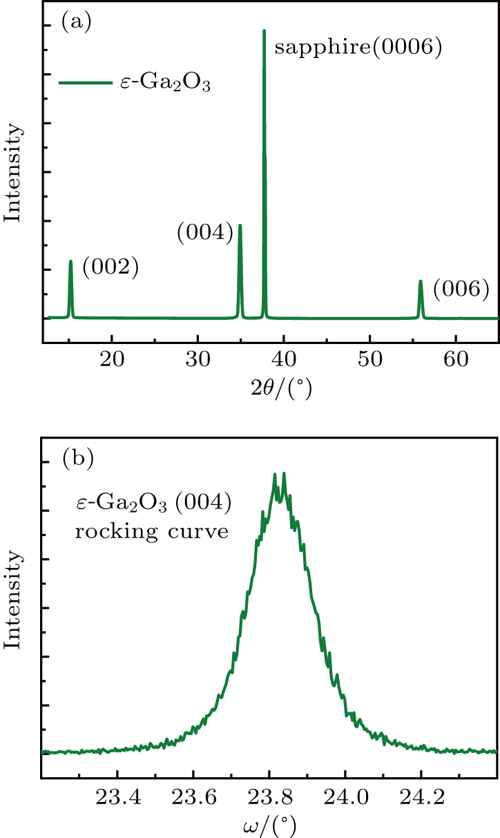
    Fig. 1. (a) The XRD pattern of the Ga2O3 thin film on c-axis sapphire substrate and (b) the rocking curve for the (004) plane.
    Cross-sectional SEM image of the ε-Ga2O3 thin film on sapphire.
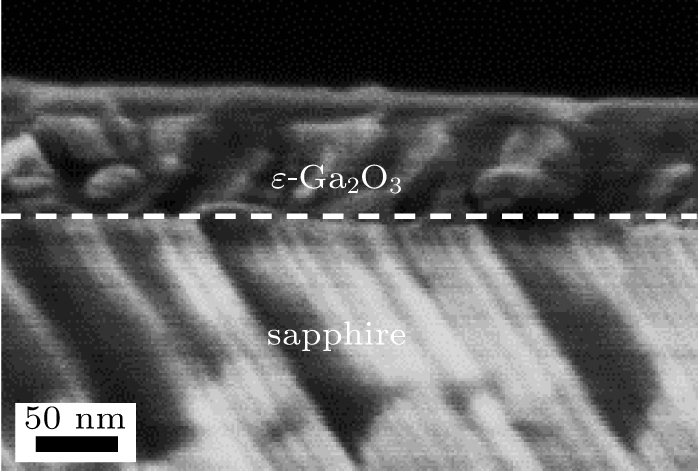
    Fig. 2. Cross-sectional SEM image of the ε-Ga2O3 thin film on sapphire.
    The transmission spectrum of the Ga2O3 thin film on c-axis sapphire substrate. The inset shows the optical bandgap calculation procedure.
    Fig. 3. The transmission spectrum of the Ga2O3 thin film on c-axis sapphire substrate. The inset shows the optical bandgap calculation procedure.
    (a) The XRD pattern and (b) transmittance spectra of the SnO thin film on glass. (c) The XRD pattern of the NiO thin film on glass, (d) the transmittance spectra of the NiO thin film on sapphire. The insets of (c) and (d) show their optical bandgaps.
    Fig. 4. (a) The XRD pattern and (b) transmittance spectra of the SnO thin film on glass. (c) The XRD pattern of the NiO thin film on glass, (d) the transmittance spectra of the NiO thin film on sapphire. The insets of (c) and (d) show their optical bandgaps.
    High resolution XPS spectra of sample 1, it shows the Ga 2p CL and VBM.
    Fig. 5. High resolution XPS spectra of sample 1, it shows the Ga 2p CL and VBM.
    High resolution XPS spectra for (a) sample 2 and (b) sample 3. (c) Schematic diagram for band alignment of the SnO/ε-Ga2O3 interface.
    Fig. 6. High resolution XPS spectra for (a) sample 2 and (b) sample 3. (c) Schematic diagram for band alignment of the SnO/ε-Ga2O3 interface.
    High resolution XPS spectra for (a) sample 4 and (b) sample 5. (c) Schematic diagram for band alignment of the NiO/ε-Ga2O3 interface.
    Fig. 7. High resolution XPS spectra for (a) sample 4 and (b) sample 5. (c) Schematic diagram for band alignment of the NiO/ε-Ga2O3 interface.
    SampleStructure
    1100 nm ε-Ga2O3 on sapphire
    275 nm SnO on glass
    33 nm SnO on ε-Ga2O3
    440 nm NiO on sapphire
    53 nm NiO on ε-Ga2O3
    Table 1. The samples.
    SampleOptical band gap/eVCL/eVVBM/eVValence band offset/eV
    SnO/ε-Ga2O314.95Ga 2p1117.61 ± 0.012.94 ± 0.022.17 ± 0.08
    22.89Sn 3d486.52 ± 0.010.77 ± 0.02
    3Ga 2p1117.61 ± 0.01
    Sn 3d486.52 ± 0.01
    NiO/ε-Ga2O314.95Ga 2p1117.61 ± 0.012.94 ± 0.021.7 ± 0.08
    43.69Ni 2p854.07 ± 0.010.63 ± 0.02
    5Ga 2p1117.39 ± 0.01
    Ni 2p854.46 ± 0.01
    Table 2. Summarize of calculation results.
    Chang Rao, Zeyuan Fei, Weiqu Chen, Zimin Chen, Xing Lu, Gang Wang, Xinzhong Wang, Jun Liang, Yanli Pei. Band alignment of p-type oxide/ε-Ga2O3 heterojunctions investigated by x-ray photoelectron spectroscopy[J]. Chinese Physics B, 2020, 29(9):
    Download Citation