Abstract
We experimentally demonstrate high-efficiency and broadband four-wave mixing in a silicon-graphene strip waveguide. A four-wave mixing conversion efficiency of and a 3-dB conversion bandwidth of 35 nm are achieved in the silicon-graphene strip waveguide with an optimized light-graphene interaction length of 60 μm. The interaction length is controlled by a windowed area of silica layer on the silicon waveguide. Numerical simulations and experimental studies are carried out and show a nonlinear parameter as large as .1. INTRODUCTION
All-optical signal processing is considered a promising technology to provide multiple high-speed signal processing functions without requiring an optical-electrical-optical conversion process [1]. Four-wave mixing (FWM), as an important parametric process, has been widely investigated to realize ultrafast all-optical signal-processing functions such as wavelength conversion [2], parametric amplification [3], optical logic gates [4], optical sampling [5], and signal regeneration [6]. Silicon photonic devices have been used to realize efficient FWM owing to the advantages of high nonlinearity, compact footprint, and compatibility with the complementary metal-oxide semiconductor (CMOS) processes [7–9]. However, the two-photon absorption (TPA) and the free-carrier absorption (FCA) effects in the silicon devices degrade the FWM conversion efficiency [10,11].
Graphene has been proved to be an excellent nonlinear optical material [12,13]. In our previous study, we demonstrated a large Kerr coefficient of graphene (), which is 6 orders of magnitude larger than that of silicon [14]. Combining graphene with silicon photonic devices offers a possible solution towards high-efficiency and broadband FWM [15,16]. Nevertheless, the high absorption of the graphene sheet greatly limits the performance of the FWM in the silicon-graphene hybrid devices [17]. The interaction length of the light with the graphene layer, which determines the device loss, needs to be precisely controlled to achieve optimal FWM efficiency. This is, however, very challenging due to the fact that the graphene sheet should be accurately sized and closely contacted with the silicon strip waveguide. Therefore, in the past, most research efforts were devoted to resonant devices, such as silicon photonics crystal cavities and microrings [18–20], since the light-graphene interactions mainly concentrated in the resonance areas. Although the conversion efficiency is enhanced with the resonance structure, the conversion bandwidth is limited by the cavity bandwidth. In this paper, we propose a design and fabrication process to accurately control the absorption loss of the graphene by defining the light-graphene interaction length in a windowed area of silica layer on the silicon waveguide. Thus the maximum net conversion efficiency can be achieved with an optimized light-graphene interaction length. The maximum conversion efficiency of the hybrid waveguide is , and the 3-dB conversion bandwidth is 35 nm, which is the widest FWM conversion bandwidth in the silicon-graphene hybrid devices to our knowledge [21], thanks to the nonresonance structure of the strip waveguide. Numerical simulations and experimental studies are carried out and show a nonlinear parameter of the graphene-on-silicon (GOS) waveguide as large as , which is 2 orders of magnitude larger than that of the silicon waveguide without graphene.
2. DEVICE DESIGN AND OPERATION PRINCIPLE
The nonlinear waveguide in our study consists of a monolayer graphene sheet on top of the silicon strip waveguide, as shown in Fig. 1(a). The cross-section view along the red dashed line is depicted in Fig. 1(b). The light-graphene interaction length is determined by a windowed silica layer on the silicon waveguide. Here, the silicon-graphene strip waveguide can be divided into two parts, i.e., the silicon waveguide under the silica layer and the GOS waveguide with the length determined by the size of the windowed silica layer. If the pump wavelength and the signal wavelength are close enough, the maximum conversion efficiency of the strip waveguide can be approximately expressed as [22] where is the nonlinear parameter, is the propagating pump power, is the effective interaction length, is the pump power coupled to the device, is the linear propagating loss coefficient, and is the geometrical length of the waveguide. Since the conversion efficiency is dependent on the nonlinear parameter, the propagating pump power, and the effective interaction length, optimizations of these parameters are needed to obtain the maximum net conversion efficiency.
Sign up for Photonics Research TOC. Get the latest issue of Photonics Research delivered right to you!Sign up now
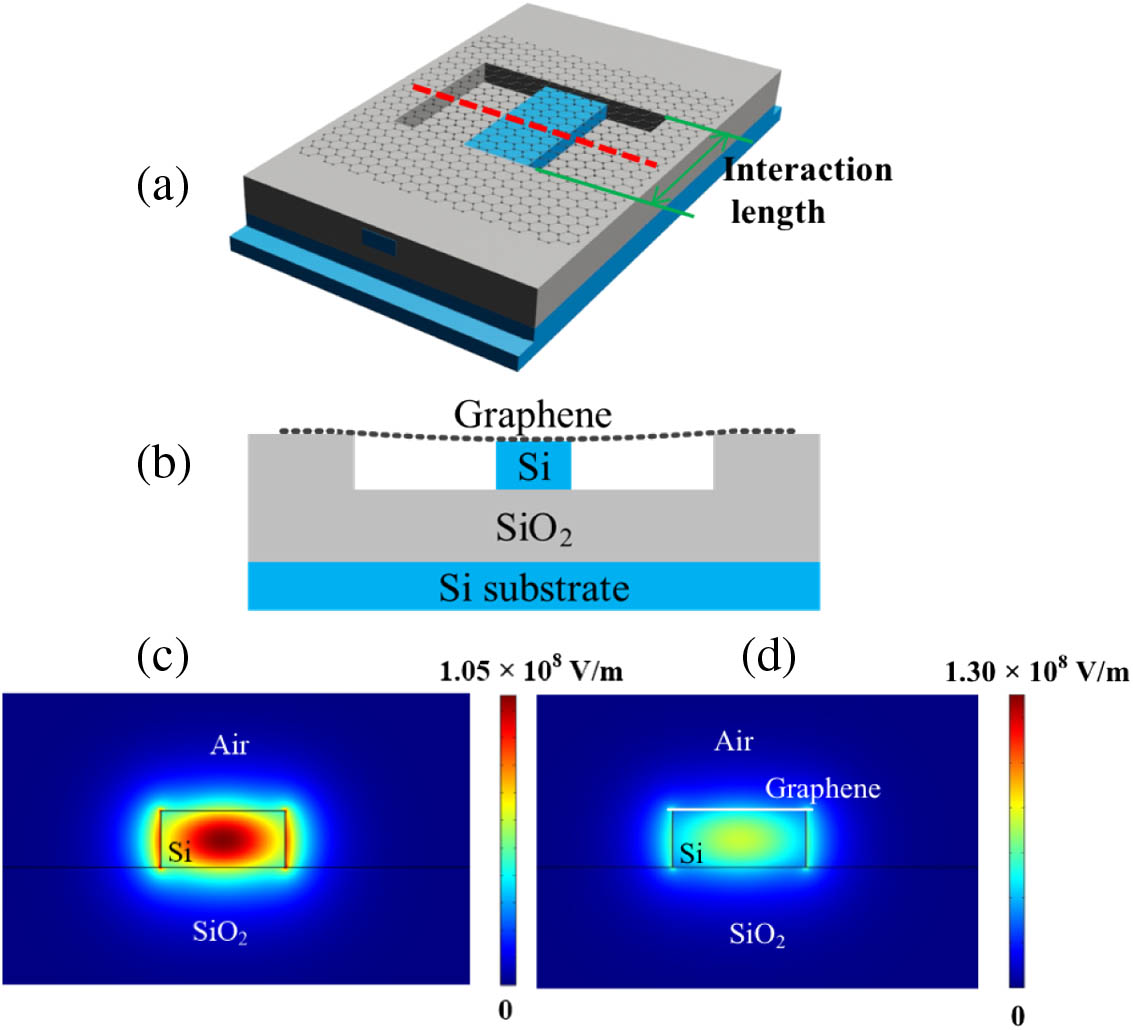
Figure 1.Structure of the proposed GOS waveguide. (a) 3D view; (b) cross-section view along the red dashed line in (a); (c) fundamental quasi-TE mode electric field distribution of the silicon waveguide; (d) fundamental quasi-TE mode electric field distribution of the GOS waveguide. The light-graphene interaction length is labeled in (a).
A numerical simulation analysis based on the finite element method (FEM) is used to investigate the enhancement of the nonlinear parameter of the GOS waveguide. Figures 1(c) and 1(d) illustrate the fundamental quasi-TE mode electric field distributions of the silicon waveguide and the proposed GOS waveguide, respectively. In the simulations, the cross section of the silicon waveguide is , and the thickness of the graphene sheet is 0.5 nm. The refractive indices of the silicon, the silica, and the graphene are set to be , , and at 1550 nm wavelength, respectively [23].
According to the modal profile, the effective nonlinear parameter is calculated by the following equation [19]: where is the time-averaged Poynting vector and is the nonlinear Kerr coefficient. The integrals are performed in the core and cladding materials with either the propagating or the evanescent electric field. The nonlinear Kerr coefficients of the silicon, the silica, and the graphene are set to be , , and , respectively [14,24,25]. Based on Eq. (4), the nonlinear parameters of the silicon waveguide and the GOS waveguide are calculated to be and , respectively. Note that the nonlinear parameter is increased by 2 orders of magnitude after transferring the graphene sheet on top of the silicon waveguide, which is similar to the results reported before [16].
The effective interaction length and the propagating pump power are greatly influenced by the linear propagating loss of the GOS waveguide, which mainly comes from the absorption of the graphene. Therefore, the maximum net conversion efficiency can be obtained by carefully controlling the light-graphene interaction length with our proposed fabrication process, which balances between the effective interaction length and the propagating pump power.
3. DEVICES FABRICATION AND RESULTS
Figure 2(a) depicts the fabrication processes of a number of silicon-graphene strip waveguides, which can be divided into four steps: (1) preparation of the silicon strip waveguides; (2) deposition of the windowed silica layer; (3) etching the chip edges for coupling; and (4) transferring the graphene sheet.

Figure 2.(a) Fabrication processes of the GOS waveguides; (b) SEM images of the GOS waveguides with different interaction lengths.
First, electron beam lithography (EBL) and inductively coupled plasma (ICP) etching were used to define the waveguides on the ZEP520A resist. The cross section and the length of the fabricated waveguide were and 3 mm, respectively. A silicon reverse taper with a 200-nm-wide tip was designed for butt-coupling. To avoid the free-space light coupling directly between the input and output fibers, the input and output waveguide ports are offset by 160 μm and connected by two quarter-circle bends with a radius of 10 μm, which are not shown in Fig. 2(a). Second, a 600-nm-thick and windowed silica layer was introduced by the EBL, depositing, and lift-off processes. This step was to control the light-graphene interaction length by patterning a silica window. Compared with patterning the graphene using the photolithography and oxygen plasma etching processes, the graphene, transferred onto the windowed silica layer, was free from the influences of contamination, wrinkles, and cracks during the fabrication processes. Thus, the loss caused by the graphene sheet is reduced. Third, lithography and deep-silicon etching processes were used to fabricate the chip edges for butt-coupling. Finally, a monolayer graphene sheet, grown with the chemical vapor deposition (CVD) approach, was transferred on top of the silicon waveguide using a poly(methyl methacrylate) (PMMA)-assisted wet-transfer method [26]. The fabricated silicon-graphene waveguides with different interaction lengths are shown by the scanning electron microscope (SEM) images in Fig. 2(b). Here, the interaction length ranges from 30 to 120 μm, which is determined by the length of the windowed silica layer on the silicon waveguides. In the experiment, the 60-μm interaction length turns out to be the optimum.
The degenerate FWM experiments with multiple GOS waveguides of different light-graphene interaction lengths were performed using the setup shown in Fig. 3(a). Two continuous-wave lights from tunable lasers are amplified by two erbium-doped fiber amplifiers (EDFAs; KEOPSYS CEFA-C-PB-HP and PriTel), which serve as the pump and signal sources, respectively. In each path, a tunable bandpass filter (BPF) and a polarization controller (PC) are employed to suppress the sideband noise of the EDFA and to ensure that the input light is TE-polarized, respectively.
Figure 3.(a) Experimental setup for testing the degenerate FWM of the fabricated devices; (b) FWM spectra of the silicon waveguide (black dashed line) and the silicon-graphene strip waveguide with a 60-μm GOS length (red solid line); insets are the zoom-in traces of the pumps and idlers.
A 50:50 coupler is used to combine the pump and the signal lights. In order to avoid damage from the reflection at the edge of the silicon waveguide, an isolator is introduced in the setup. Then the light is coupled into and out of the device under test (DUT) through two lensed fibers with a coupling loss of 6.7 dB/facet. For the silicon waveguide, the linear propagating loss is 3.6 dB/cm. The output light is detected by the optical spectrum analyzer (OSA; Yokogawa, AQ6370). For the TM polarization, the electric field is less confined in the device; thus it is sensitive to device imperfections. Therefore, only the TE polarization is used in our study.
Here the conversion efficiency of the FWM is defined as the ratio of output idler power to the input signal power [3]. After being coupled into the device, the pump power is 13.8 dBm at 1550 nm, and the signal power is 3.8 dBm at 1549.5 nm. The output power spectra of the silicon waveguide and the silicon-graphene strip waveguide are plotted in Fig. 3(b). The idler power at the end of the silicon-graphene strip waveguide is , with an output coupling loss of 6.7 dB. Thus, the measured maximum conversion efficiency is by excluding the coupling loss. For the silicon-graphene strip waveguide, the total length of the silicon waveguide is 3 mm, and the optimum light-graphene interaction length is 60 μm. Compared with the 3-mm-long silicon waveguide without graphene, the conversion efficiency of the GOS waveguide is increased by 4.8 dB, as shown in the inset of Fig. 3(b).
If the input pump power is increased from 2.8 to 13.8 dBm, the conversion efficiencies of the silicon waveguide and the GOS waveguide increase linearly with the similar slopes of , as shown in Fig. 4(a), indicating that the nonlinear absorptions and nonlinear losses are not significant in the FWM processes [21,27]. The calculated conversion efficiencies based on Eqs. (1)–(3) are also plotted in Fig. 4(a). Equation (1) neglects the phase mismatch if the pump wavelength and the signal wavelength are close enough, while the wavelength spacing between the pump and the signal lights is 0.5 nm in the experiment. Thus, small discrepancies between the experimental results and the theoretical results of the two waveguides are observed. For the silicon-graphene strip waveguide, a detectable idler can be produced with a pump power of 2.8 dBm, showing the high nonlinearity of the GOS waveguide. Here, the conversion processes in the nonlinear waveguide come from two parts, i.e., the nonlinear conversion from the silicon waveguide under the silica layer and that from the GOS waveguide. To characterize the FWM performance of the 3-mm-long nonlinear waveguide, the nonlinear parameters and the figures of merit [28] for the two waveguides are obtained, respectively, by Eqs. (1)–(3). Based on the experimental results, and are calculated to be and , respectively. The figure of merit, , is and for the silicon waveguide and the GOS waveguide, respectively. Thus the conversion efficiency is mainly contributed by the GOS waveguide.
Figure 4.(a) Experimental and calculated conversion efficiencies of the silicon waveguide and the silicon-graphene strip waveguide versus the input pump power; (b) experimental conversion efficiencies of the silicon waveguide (black circle) and the silicon-graphene strip waveguide (red square) versus the signal wavelength; calculated conversion efficiency of the silicon-graphene strip waveguide (blue solid line) versus the signal wavelength.
Figure 4(b) shows the conversion efficiency versus the signal wavelength when the pump wavelength is fixed at 1550 nm and the input power is 13.8 dB. The 3-dB conversion bandwidths of the silicon waveguide and the silicon-graphene strip waveguide are 9 and 35 nm, respectively. The conversion efficiency and the bandwidth of the FWM process are affected by the interaction length of the waveguide and wave vector mismatch between the pump and signal lights [7]. Since the thickness of the graphene layer is only 0.5 nm, the difference of the effective refraction indices between the GOS waveguide and the silicon waveguide is negligible, according to the simulated results. Thus, the wave vector mismatch is mainly produced by the propagation in the waveguide.
With longer interaction length, the mismatch of the wave vector between the pump and signal lights is more severe, which leads to a narrower conversion bandwidth [27]. Although in the device the length of the silicon waveguide under the silica layer is 2.94 mm, the conversion efficiency and the bandwidth of the device are mostly determined by the GOS waveguide, where the highly nonlinear process happens. In the example of 60-μm light-graphene interaction length, such a short interaction length would not produce significant wave vector mismatch, while for the silicon waveguide without graphene, the conversion takes place in the 3-mm-long silicon waveguide, resulting in a larger wave vector mismatch. As a result, a broadband conversion bandwidth is achieved in the GOS waveguide. The operation wavelengths of the two lasers are limited in the C-band, and no obvious roll-off of the conversion spectrum is observed. The bandwidth of the GOS waveguide is theoretically calculated by taking into the second- and fourth-order dispersion effects as described in Ref. [7]. A 3-dB conversion bandwidth of 140 nm is expected.
The absorption loss of the graphene layer is measured with the cutback method. By changing the lengths of the windowed silica layer on the silicon waveguides, the lengths of the GOS waveguides range from 30 to 120 μm with a 30-μm step size. The measured absorption losses of the graphene are provided in Fig. 5(a). The absorption loss varies proportionally with the GOS waveguide length, indicating the effectiveness by introducing the windowed silica layer. According to the fitted result, the absorption coefficient of the GOS waveguide is 0.03 dB/μm.
Figure 5.(a) Absorption loss of the graphene sheet versus the length of the GOS waveguide; (b) conversion efficiency of the silicon-graphene strip waveguide versus the length of the GOS waveguide.
In Fig. 5(b), the conversion efficiencies of the silicon-graphene strip waveguides with different GOS waveguide lengths are plotted. The experimental results show that the conversion efficiency first increases with the interaction length, and then decreases at the longer interaction lengths due to the absorption loss. The maximum conversion efficiency of at an optimum GOS waveguide length of 60 μm is achieved in our study. Since the TPA coefficient of the GOS waveguide is assumed to be 25 cm/GW [18], the conversion efficiency can be enhanced by further increasing the pump power.
Table 1 provides comparisons of our work versus several recently reported devices on CMOS platforms. In our work, the GOS waveguide enables a high conversion efficiency and broad bandwidth due to a large of the GOS waveguide.
| Device | Conversion Efficiency | Bandwidth | Length | Pump Power | Nonlinear Coefficient |
| PhC cavity [18] | −30 dB | ∼200 pm | 0.12 mm | 600 μW | n2=4.8×10⁻¹⁷ m2/W |
| PhcWG [21] | −23 dB | 17 nm | 200 μm | 17 dBm | n2=4.8×10⁻¹⁷ m2/W |
| SGM [19] | −37 dB | – | – | 8 mW | n2=1.5×10¹⁷ m2/W |
| SiNX waveguide [29] | −46 dB | >16 nm | 8 mm | 10 dBm | n2=3×10⁻¹⁸ m2/W |
| Si7N3 waveguide [30] | −40 dB | >90 nm | 7 mm | 4.7 dBm | n2=2.8×10⁻¹⁷ m2/W |
| USRN waveguide [31] | 27 dB | ∼100 nm | 10 mm | 26 W | γ=330 W−1·m−1 |
| Our work | −38.7 dB | >35 nm (experimental) ∼140 nm (calculated) | 3 mm (60-μm GOS) | 13.8 dBm | γGOS=1.0×10⁴ W−1·m−1 |
Table 1. Characteristics of FWM Process for Devices on CMOS Platformsa
4. CONCLUSION
In summary, we have experimentally demonstrated high-efficiency and broadband FWM using the silicon-graphene strip waveguide by accurately controlling the light-graphene interaction length. A conversion efficiency of and a 3-dB conversion bandwidth of 35 nm are achieved using a GOS waveguide with an optimal 60-μm interaction length. The nonlinear parameter of the GOS waveguide, which is as large as , is calculated from experimental results and numerical simulations. The proposed GOS waveguide offers a new possibility for future high-speed and large-capacity all-optical signal processing.
Acknowledgment
Acknowledgment. We thank the center for Advanced Electronic Materials and Devices (AEMD) of Shanghai Jiao Tong University for the support in device fabrication and characterization.
References
[1] A. E. Willner, M. R. Chitgarha, O. F. Yilmaz. All-optical signal processing. J. Lightwave Technol., 32, 660-680(2014).
[2] S. Gao, E.-K. Tien, Q. Song, Y. Huang, O. Boyraz. Ultra-broadband one-to-two wavelength conversion using low-phase-mismatching four-wave mixing in silicon waveguides. Opt. Express, 18, 11898-11903(2010).
[3] M. A. Foster, A. C. Turner, J. E. Sharping, B. S. Schmidt, M. Lipson, A. L. Gaeta. Broad-band optical parametric gain on a silicon photonic chip. Nature, 441, 960-963(2006).
[4] Z. Li, G. Li. Ultrahigh-speed reconfigurable logic gates based on four-wave mixing in a semiconductor optical amplifier. IEEE Photon. Technol. Lett., 18, 1341-1343(2006).
[5] J. V. Erps, F. Luan, M. D. Pelusi, T. Iredale, S. Madden, D.-Y. Choi, D. A. Bulla, B. Luther-Davies, H. Thienpont, B. J. Eggleton. High-resolution optical sampling of 640-Gb/s Data. J. Lightwave Technol., 28, 209-215(2010).
[6] R. Salem, M. A. Foster, A. C. Turner, D. F. Geraghty, M. Lipson, A. L. Gaeta. Signal regeneration using low-power four-wave mixing on silicon chip. Nat. Photonics, 2, 35-38(2008).
[7] M. A. Foster, A. C. Turner, R. Salem, M. Lipson, A. L. Gaeta. Broad-band continuous-wave parametric wavelength conversion in silicon nanowaveguides. Opt. Express, 15, 12949-12958(2007).
[8] L. Thylén, L. Wosinski. Integrated photonics in the 21st century. Photon. Res., 2, 75-81(2014).
[9] Z. Zhou, B. Yin, Q. Deng, X. Li, J. Cui. Lowering the energy consumption in silicon photonic devices and systems. Photon. Res., 3, B28-B46(2015).
[10] J. Leuthold, C. Koos, W. Freude. Nonlinear silicon photonics. Nat. Photonics, 4, 535-544(2010).
[11] C. Koos, P. Vorreau, T. Vallaitis, P. Dumon, W. Bogaerts, R. Baets, B. Esembeson, I. Biaggio, T. Michinobu, F. Diederich, W. Freude, J. Leuthold. All-optical high-speed signal processing with silicon-organic hybrid slot waveguides. Nat. Photonics, 3, 216-219(2009).
[12] L. Miao, Y. Jiang, S. Lu, B. Shi, C. Zhao, H. Zhang, S. Wen. Broadband ultrafast nonlinear optical response of few-layers graphene: toward the mid-infrared regime. Photon. Res., 3, 214-219(2015).
[13] E. Hendry, P. J. Hale, J. Moger, A. K. Savchenko, S. A. Mikhailov. Coherent nonlinear optical response of graphene. Phys. Rev. Lett., 105, 097401(2010).
[14] Y. Yang, R. Liu, J. Wu, X. Jiang, P. Cao, X. Hu, T. Pan, C. Qiu, J. Yang, Y. Song, D. Wu, Y. Su. Bottom-up fabrication of graphene on silicon/silica substrate via a facile soft-hard template approach. Sci. Rep., 5, 13480(2015).
[15] N. Vermeulen, J. Cheng, J. E. Sipe, H. Thienpont. Opportunities for wideband wavelength conversion in foundry-compatible silicon waveguides covered with graphene. IEEE J. Sel. Top. Quantum Electron., 22, 347-359(2016).
[16] C. Donnelly, D. T. H. Tan. Ultra-large nonlinear parameter in graphene-silicon waveguide structures. Opt. Express, 22, 22820-22830(2014).
[17] H. Li, Y. Anugrah, S. J. Koester, M. Li. Optical absorption in graphene integrated on silicon waveguides. Appl. Phys. Lett., 101, 111110(2012).
[18] T. Gu, N. Petrone, J. F. McMillan, A. van der Zande, M. Yu, G. Q. Lo, D. L. Kwong, J. Hone, C. W. Wong. Regenerative oscillation and four-wave mixing in graphene optoelectronics. Nat. Photonics, 6, 554-559(2012).
[19] M. Ji, H. Cai, L. Deng, Y. Huang, Q. Huang, J. Xia, Z. Li, J. Yu, Y. Wang. Enhanced parametric frequency conversion in a compact silicon-graphene microring resonator. Opt. Express, 23, 18679-18685(2015).
[20] X. Hu, Y. Long, M. Ji, A. Wang, L. Zhu, Z. Ruan, Y. Wang, J. Wang. Graphene-silicon microring resonator enhanced all-optical up and down wavelength conversion of QPSK signal. Opt. Express, 24, 7168-7177(2016).
[21] H. Zhou, T. Gu, J. F. McMillan, N. Petrone, A. van der Zande, J. C. Hone, M. Yu, G. Lo, D.-L. Kwong, G. Feng, S. Zhou, C. W. Wong. Enhanced four-wave mixing in graphene-silicon slow-light photonic crystal waveguides. Appl. Phys. Lett., 105, 091111(2014).
[22] K. K. Chow, S. Yamashita, S. Y. Set. Four-wave-mixing-based wavelength conversion using a single-walled carbon-nanotube-deposited planar lightwave circuit waveguide. Opt. Lett., 35, 2070-2072(2010).
[23] K. J. A. Ooi, L. K. Ang, D. T. H. Tan. Waveguide engineering of graphene’s nonlinearity. Appl. Phys. Lett., 105, 111110(2014).
[24] M. Dinu, F. Quochi, H. Garcia. Third-order nonlinearities in silicon at telecom wavelengths. Appl. Phys. Lett., 82, 2954-2956(2003).
[25] H. R. K. J. Vahala. Observation of Kerr nonlinearity in microcavities at room temperature. Opt. Lett., 30, 427-429(2005).
[26] X. Liang, B. A. Sperling, I. Calizo, G. Cheng, C. A. Hacker, Q. Zhang, Y. Obeng, K. Yan, H. Peng, Q. Li, X. Zhu, H. Yuan, A. R. H. Walker, Z. Liu, L.-M. Peng, C. A. Richter. Toward clean and crackless transfer of graphene. ACS Nano, 5, 9144-9153(2011).
[27] H. Fukuda, K. Yamada, T. Shoji, M. Takahashi, T. Tsuchizawa, T. Watanabe, J. Takahashi, S. Itabashi. Four-wave mixing in silicon wire waveguides. Opt. Express, 13, 4629-4637(2005).
[28] D. T. H. Tan, K. J. A. Ooi, D. K. T. Ng. Nonlinear optics on silicon-rich nitride—a high nonlinear figure of merit CMOS platform. Photon. Res., 6, B50-B66(2018).
[29] C.-L. Wu, Y.-H. Lin, S.-P. Su, B.-J. Huang, G.-R. Lin. Degenerate four-wave mixing in Si quantum dot doped Si-rich SiNx channel waveguide. J. Lightwave Technol., 34, 4110-4119(2016).
[30] K. J. Ooi, D. K. T. Ng, T. Wang, A. K. L. Chee, S. K. Ng, L. K. Ang, A. M. Agarwal, L. C. Kimerling, D. T. H. Tan. Pushing the limits of CMOS optical parametric amplifiers with USRN:Si7N3 above the two-photon absorption edge. Nat. Commun., 8, 13878(2017).
[31] J. W. Choi, B.-U. Sohn, G. F. R. Chen, D. K. T. Ng, D. T. H. Tan. Broadband incoherent four-wave mixing and 27 dB idler conversion efficiency using ultra-silicon rich nitride devices. Appl. Phys. Lett., 112, 181101(2018).


