
Yang Song, Xi-Bin Yang, Bing Yan, Chi Wang, Jian-Mei Sun, Da-Xi Xiong. Super-resolution imaging system based on integrated microsphere objective lens [J]. Acta Physica Sinica, 2020, 69(13): 134201-1
- Acta Physica Sinica
- Vol. 69, Issue 13, 134201-1 (2020)
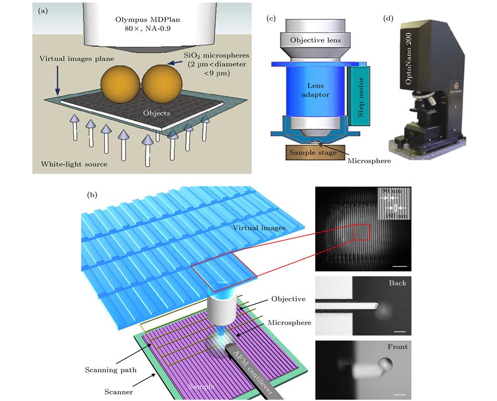
Fig. 1. (a) Schematic of spread the microspheres; (b) Schematic of AFM probes control microspheres; (c) The universal lens adaptor for the microsphere; (d)Microsphere assisted microscopy OptoNano 200.
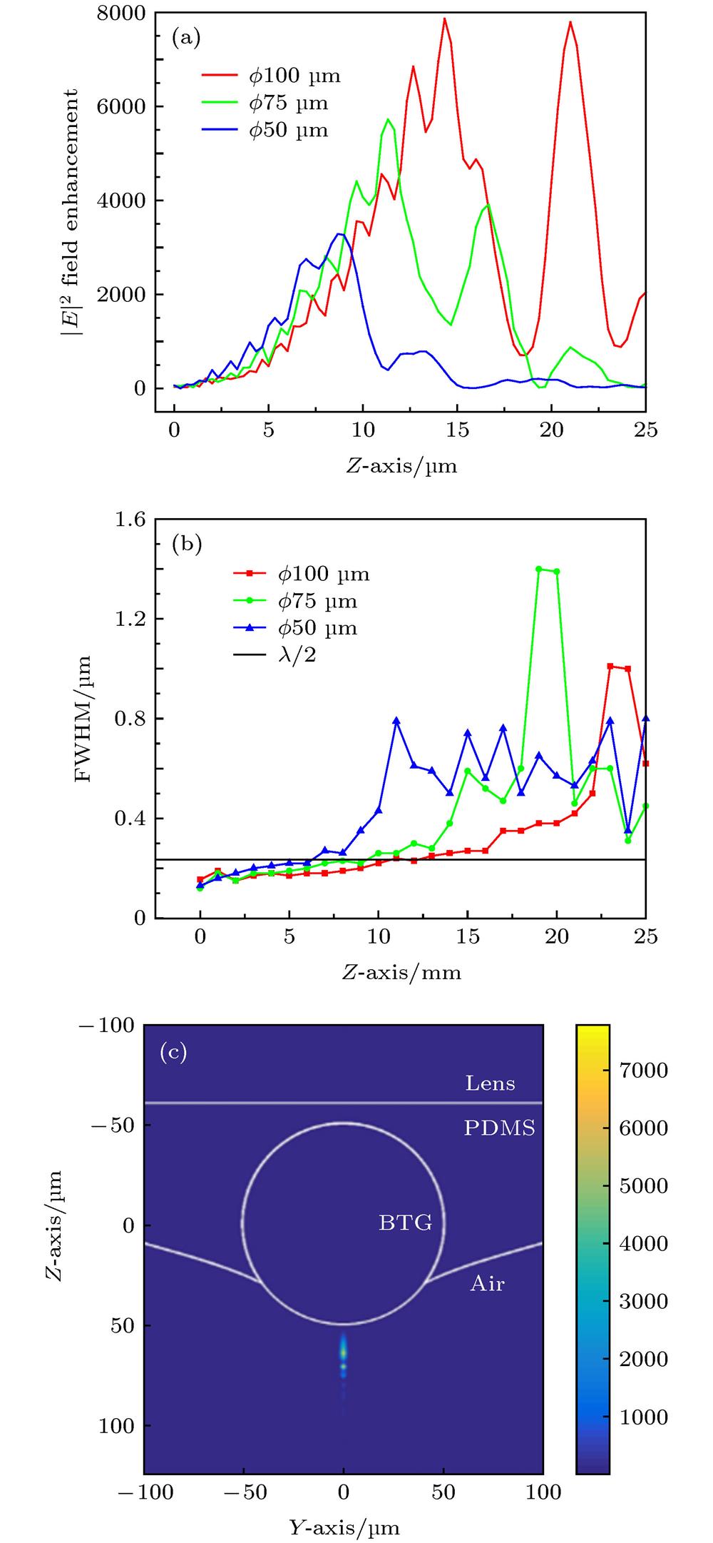
Fig. 2. (a) Intensity curve value in Z -axis direction of the photonic nanojet formed by BTG microspheres with diameters of 50, 75 and 100 μm; (b) FWHM of the photonic nanojet formed by BTG microspheres; (c) The photonic nanojet formed by 100 μm microspheres at the wavelength of 470 nm.
Fig. 3. Schematic and experimental set-up diagram of microsphere imaging system.
Fig. 4. (a) Physical image of the super-resolution microsphere objective; (b) Fabrication of the super-resolution microsphere objective lens. It mainly includes 1) sleeves, 2) coating of PDMS, 3) adhesion of microspheres, 4) integrated objective lens; (c) Physical image of side-view imaging and position feedback system; (d) Adhesion of microspheres. It mainly includes 1) positioning of microspheres, 2) downward of the lens, 3) adhesion of microspheres, 4) downward of the displacement table.
Fig. 5. (a) Calibration of side-view imaging feedback system; (b) An example of microsphere lens working at a distance of 12.65 μm.
Fig. 6. (a) The CPU lattice structure, 400 nm blocks and 200 nm intervals, observed by scanning electron microscope (SEM); (b) the observation without microsphere lens; (c)−(h) the lattice observed at the working distance of 2.78, 4.63, 5.55, 7.72, 9.57 and 12.65 μm, respectively, with 100 μm diameter microspheres. The left side of each group of images is the microscopic image, in which the field of view is inside the white circle, the gray value change curve at the diameter (the white line) is shown in the lower right corner, and the upper right corner is the corresponding side-view images. All of them can effectively distinguish 200 nm lattice features; (i) the relationship curve between the magnification factor and the working distance of the microsphere.
Fig. 7. (a) The BD-ROM fringe observed by scanning electron microscope (SEM); (b) the observation without microsphere lens; (c) the observation with microsphere lens. The left side of image is the microscopic image, the BD-ROM fringe can be observed clearly, in which the field of view is inside the white circle, the gray value change curve at the diameter (the white line) is shown in the lower right corner, and the upper right corner is the corresponding side-view images. The working distance is about 3 μm and the field of view is about 8.04 μm2.

Set citation alerts for the article
Please enter your email address
© Copyright 2018-2021 | Chinese Laser Press. All Rights Reserved 沪ICP备15018463号-20