• Acta Photonica Sinica
  • Vol. 50, Issue 5, 43 (2021)
Hongjie DING1, Peng LIU1, Yong LIU2, Hong CHANG2, Shouqian CHEN3, and Wang ZHANG1
Author Affiliations
  • 1School of Mechanical and Aerospace Engineering, Jilin University,Changchun30022, China
  • 2Beijing Aerospace Institute for Metrology and Measurement Technology, Beijing100076,China
  • 3Research Center for Space Optical Engineering, Harbin Institute of Technology, Harbin150001,China
  • show less
    DOI: 10.3788/gzxb20215005.0513001 Cite this Article
    Hongjie DING, Peng LIU, Yong LIU, Hong CHANG, Shouqian CHEN, Wang ZHANG. Research on Designing Approaches for Device and Integration of Photonic Integrated Interferometric Detecting System[J]. Acta Photonica Sinica, 2021, 50(5): 43 Copy Citation Text show less
    Schematic diagram of the PIC
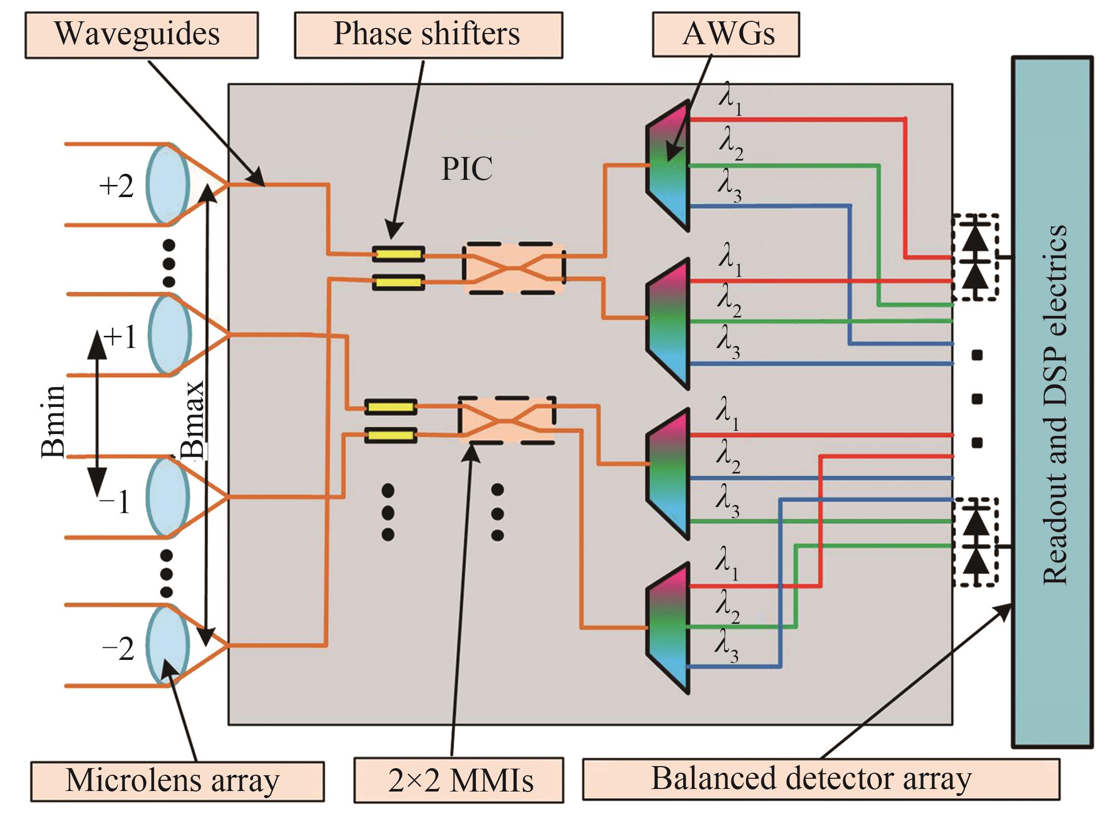
    Fig. 1. Schematic diagram of the PIC
    Crosstalk between adjacent optical waveguides
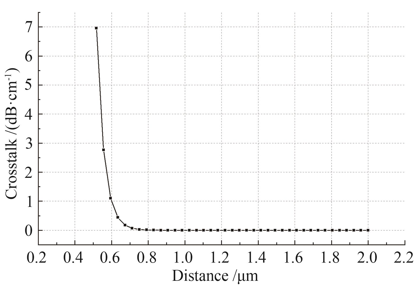
    Fig. 2. Crosstalk between adjacent optical waveguides
    Loss of bent waveguide
    Fig. 3. Loss of bent waveguide
    1×16 AWG simulation results
    Fig. 4. 1×16 AWG simulation results
    Temperature distribution of phase modulator simulation model
    Fig. 5. Temperature distribution of phase modulator simulation model
    Time response for π phase shift
    Fig. 6. Time response for π phase shift
    The relationship between the thickness of the upper cladding layer and the metal absorption loss
    Fig. 7. The relationship between the thickness of the upper cladding layer and the metal absorption loss
    Improved MMI simulation results
    Fig. 8. Improved MMI simulation results
    Results of multi-layer waveguide
    Fig. 9. Results of multi-layer waveguide
    Layout of photonic integrated chip
    Fig. 10. Layout of photonic integrated chip
    Schematic of Si waveguides
    Fig. 11. Schematic of Si waveguides
    Bending loss of Si3N4 waveguide
    Fig. 12. Bending loss of Si3N4 waveguide
    Structural diagram of the interlayer transition of waveguides
    Fig. 13. Structural diagram of the interlayer transition of waveguides
    Overall layout of photonic integrated chip
    Fig. 14. Overall layout of photonic integrated chip
    interference baselines on different Lens Pairs
    Fig. 15. interference baselines on different Lens Pairs
    Schematic of focal plane and multi-waveguides
    Fig. 16. Schematic of focal plane and multi-waveguides
    Schematic diagram of three-dimensional simulation of electronic prototype
    Fig. 17. Schematic diagram of three-dimensional simulation of electronic prototype
    Design parameterSymbolValue
    Center wavelengthλ01.56 μm
    Index of planar waveguidens2.84
    Index of rectangular waveguidenc2.48
    Number of armsM60
    Free spectral regionFSR51.2 nm
    Grating orderm30
    Number of input/output waveguidesN1×16
    Channel spacingd3.2 nm
    Table 1. Design parameter table of 1×3AWG
    Design parameterSymbolValue
    Longest baselineBmax30.4 mm
    Wavelengthλ1.53~1.59 μm
    Diameter of microlensd1 mm
    Number of microlensesK16
    Field of viewθ0.5 °
    Focal lengthf1 mm
    Table 2. Microlens interference baseline design index
    Design parameterSymbolValue
    PIC cardsNz41
    Prototype caliberΦ110 mm
    Wavelengthλ1.53~1.59 μm
    Field of viewθ0.5 °
    Observation distanceZ100 km
    Spatial resolutionδ05 m
    Angular resolutionδ10.05 mrad
    Diameter of microlensd1 mm
    Spectral numberNq16(Δλ=3.2 nm)
    Table 3. Design parameters of the simulation electronic prototype
    Hongjie DING, Peng LIU, Yong LIU, Hong CHANG, Shouqian CHEN, Wang ZHANG. Research on Designing Approaches for Device and Integration of Photonic Integrated Interferometric Detecting System[J]. Acta Photonica Sinica, 2021, 50(5): 43
    Download Citation