• Photonics Research
  • Vol. 10, Issue 8, 1886 (2022)
Zihao Shuang1、2、3, Hai Zhou1、3、4、*, Dingjun Wu2、3, Xuhui Zhang2、3, Boao Xiao2、3, Jinxia Duan2、3, and Hao Wang2、3、5、*
Author Affiliations
  • 1International School of Microelectronics, Dongguan University of Technology, Dongguan 523808, China
  • 2Hubei Yangtze Memory Laboratories, Wuhan 430205, China
  • 3School of Microelectronics, Hubei University, Wuhan 430062, China
  • 4e-mail: hizhou@dgut.edu.cn
  • 5e-mail: wangh@hubu.edu.cn
  • show less
    DOI: 10.1364/PRJ.452883 Cite this Article Set citation alerts
    Zihao Shuang, Hai Zhou, Dingjun Wu, Xuhui Zhang, Boao Xiao, Jinxia Duan, Hao Wang. High-performance Ag2BiI5 Pb-free perovskite photodetector[J]. Photonics Research, 2022, 10(8): 1886 Copy Citation Text show less

    Abstract

    Recently, lead-free all-inorganic halide perovskites have attracted great interest because they not only have the merits of the halide perovskite family, but also are non-toxic. However, the commercialization of lead-free all-inorganic perovskites is restricted by their relatively low performances, which are usually caused by the fabrication methods and undesirable interfaces between the active layer and carrier transport layers. Herein, we demonstrate a solution-processed route for high-quality Ag2BiI5 lead-free perovskite film by adopting ideal electron transport material SnO2 and a carbon electrode. By optimizing the fabrication process and tailoring the composition of the perovskite active layer, a high-performance photodetector (PD) with an FTO/SnO2/Ag2BiI5/carbon structure PD is first fabricated, which shows good self-powered performance with a detectivity of as high as 5.3×10¹² Jones and a linear dynamic range of up to 138 dB, which are better than those of the reported Pb-free perovskite PDs and comparable to high-performance Pb-based perovskite PDs. In addition, our unpackaged PDs show good light, thermal, and storage stability in air. Our results provide a special route for the development of lead-free perovskite devices in an environmentally friendly field.

    1. INTRODUCTION

    Organic–inorganic hybrid lead halide perovskite materials have shown great achievements in the field of optoelectronic devices due to their large light absorption coefficient, low defect state density, and high carrier mobility [13]. At the same time, a simple solution spin-coating method can prepare high-quality films, which greatly reduces cost and promotes commercial application [4]. However, the thermal instability of organic–inorganic hybrid lead halide perovskite materials and the toxicity of lead limit their large-scale application. Therefore, seeking highly stable and environmentally friendly perovskite materials has become a research hotspot [5,6]. Different from traditional ABX3-type perovskite composed of angle-sharing [BX6] octahedrons [where A is a monovalent inorganic cation (Cs+, Rb+) or an organic ion group (CH3NH3+, NH2CHNH2+), B is a divalent metal cation, and X is monovalent anions (I, Br, and Cl)], a new halide photovoltaic material based on edge sharing [AX6] and [CX6] octahedrons provides an idea for replacing Pb in perovskites. Monovalent cations and trivalent cations combine to form AaCbXa+3b perovskite (A: Ag, Cu; C: Bi, Sb; X: I, Br), which alternately share [AX6] and [CX6] octahedrons (Ivan Turkevych named this structure as “rudorffites”) [7]. As a representative of the AaCbXa+3b perovskite, AgaBibIx (x=a+3b) is considered to be a promising material. The rapid increase in power conversion efficiency in the field of solar cells has proved their development potential [810], but their current device performances are not high and are restricted by fabrication methods and undesirable interfaces between the active layer and carrier transport layers. Therefore, exploring new methods and device structure to improve device performance is essential.

    The performance of non-lead perovskite devices is greatly affected by the crystal quality of perovskite films [11,12]. Since most lead-free stabilized perovskite materials are all-inorganic, their thin-film crystal quality is more easily affected by the material preparation process. Among these processes, thermal evaporation is often used to fabricate all-inorganic lead-free perovskites, mainly because of the uniformity and high quality of the prepared films [13]. For example, Huabin Lan and co-authors prepared all-inorganic lead-free perovskite CsBi3I10 thin films by single-source thermal evaporation deposition; the film surface was compact and uniform, and had high homology with the crystal structure of the evaporation source material [14]. However, the use of thermal evaporation will cause great waste of materials, which is not conducive to commercialization. As a widely used solution spin-coating method in Pb-based perovskite devices, although it has the advantages of simple preparation and high utilization rate of raw materials, it is difficult to prepare all-inorganic non-lead perovskites due to the low solubility of the precursors in organic solvent and the poor film quality [15,16]. Therefore, a series of improved spin-coating methods have been developed, such as hot spin-coating, anti-solvent assisted method, and step-by-step annealing [1719]. In addition, the use of excellent transport layer materials not only utilizes the transport and separation of photogenerated carriers, but also facilitates the growth of thin-film crystal quality, and ultimately enables the device to obtain excellent optoelectronic properties [20]. For example, according to Dong Yang and co-authors’ work, the record power conversion efficiency of planar-type perovskite solar cells with ethylene diamine tetraacetic acid-complexed SnO2 increases to 21.60% with negligible hysteresis [21].

    Herein, we first introduce SnO2 as an electron transport layer (ETL) to fabricate high-quality lead-free Ag2BiI5 perovskite film by a hot-spin-coating route. Compared with other ETLs, SnO2 has the following merits: (1) good energy level and high electron mobility (up to 240  cm2V1s1), which will enhance electron extraction and hole blocking, reducing the recombination loss, and improving the electron transport efficiency; (2) high transmittance over the whole visible spectra, which will allow most light to pass through ETL and be absorbed by perovskite active layer; (3) compared to TiO2 or other ETL, SnO2 displays excellent UV-resistance properties, chemical stability, and less photocatalytic activity, which will improve the stability of the device. By optimizing the fabrication process and tailoring the composition of the perovskite active layer, the crystal quality and light absorption of the Ag2BiI5 film were optimized, and a self-powered photodetector (PD) with the fluorine-doped tin oxide (FTO)/SnO2/Ag2BiI5/carbon structure was fabricated. Finally, our optimized Ag2BiI5 PDs achieved good detection capability for weak light. Under a 473 nm laser with a light intensity of 34  nW/cm2, our PD showed detectivity (D*) as high as 5.3×10¹² Jones and a linear dynamic range (LDR) of up to 138 dB. In addition, our unpackaged PDs showed good light, thermal, and storage stability in air. Our results provide a special route for the development of lead-free perovskite devices in an environmentally friendly field.

    2. EXPERIMENT

    A. Preparation of SnO2 Film

    First, the FTO glass was cleaned by using deionized water, acetone, and alcohol. We mixed 15% (mass fraction) SnO2 syrup and deionized water at a volume ratio of 1:4 and ultrasonically for 10 min. After that, 100 μL of SnO2 aqueous solution was spin-coated at 3000 r/min on the surface of FTO, and then annealed at 150°C for 30 min.

    B. Fabrication of Ag2BiI5 Thin-Film Devices

    We dissolved AgI powder and BiI3 powder in a 2:1 ratio in a mixed solution of dimethyl sulfoxide (DMSO) and N, N-dimethylformamide (DMF) to prepare a 0.3 M (1  M=1mol/L) Ag2BiI5 precursor solution (DMF:DMSO=3:1), and stirred completely to get a clear and transparent solution. We filtered the solution through a polytetrafluoroethylene (PTFE) syringe filter (0.45 μm). The SnO2 coated FTO substrate and Ag2BiI5 solution were simultaneously preheated at 100°C, and then 80 μL of the solution was spin-coated on the FTO at 5000 r/min, and finally annealed at 190°C for 10 min.

    Finally, a layer of carbon paste was scraped on the surface of the Ag2BiI5 film and annealed at 120°C for 15 min to prepare a complete device.

    C. Characterization

    High-resolution SEM images, X-ray diffraction (XRD) patterns, and absorption spectra were recorded by field emission SEM (FESEM, JEOL, JSM-6700F), a D8 FOCUS X-ray diffractometer, and a UV-Vis spectrophotometer, respectively. A Keithley 2400 source meter was used to record current–voltage (I-V) and current–time (I-t) curves. An oscilloscope was used to characterize the fast response time of our devices. A 473 nm laser was used as the light source, and its optical power was calibrated by a standard Si diode. A time-correlated single-photon counting technique (Fluo-Time 300, Pico Quant GmbH) was used to measure the time-resolved photoluminescence (TRPL) decay spectra of the samples.

    3. RESULTS AND DISCUSSION

    Figure 1(a) shows the electronic structure of Ag2BiI5 perovskite, which indicates AgI and BiI3 regular octahedrons alternately share edges. To optimize the surface morphology and quality of the Ag2BiI5 perovskite film, we first study the influence of the precursor concentration on the morphology of the perovskite film, as shown in Figs. 1(b)–1(f). The 0.2–0.6 M Ag2BiI5 precursor solution is spin-coated at 5000 r/min, and the corresponding SEM images are shown in Figs. 1(b)–1(f). It can be seen that as the concentration of the precursor increases, the grain size of the perovskite first increases and then decreases; the largest grain size of the perovskite can reach as big as 500 nm and no holes can be seen, which is better than other reports [22,23] and may be attributed to the SnO2 ETL. In addition, there are large particles among the perovskite grains, and as the concentration increases (0.3–0.5 M), the particles increase in size and quantity; these particles should be BiI3, which can be verified by X-ray photoelectron spectroscopy (XPS), shown in Figs. 1(g)–1(i). From the figures, we can calculate a ratio of Ag:Bi:I=19.04:19.65:61.31, indicating that many Bi and I elements exist on the surface of the perovskite.

    Characteristics of Ag2BiI5 films with different precursor concentrations: (a) Ag2BiI5 electronic structure diagram; (b)–(f) SEM morphologies of Ag2BiI5 films prepared by 0.2–0.6 M precursor concentrations; (g)–(i) XPS high-resolution spectra of the perovskite surface analysis.

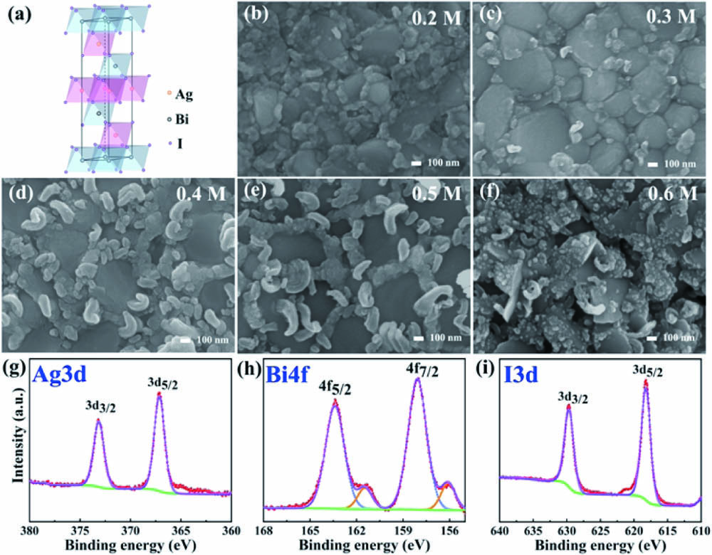
    Figure 1.Characteristics of Ag2BiI5 films with different precursor concentrations: (a) Ag2BiI5 electronic structure diagram; (b)–(f) SEM morphologies of Ag2BiI5 films prepared by 0.2–0.6 M precursor concentrations; (g)–(i) XPS high-resolution spectra of the perovskite surface analysis.

    Figure 2(a) shows the XRD patterns of the Ag2BiI5 perovskite films, and all of the curves indicate a strong (003) diffraction peak with few weak peaks, which is consistent with the reported Ag2BiI5 perovskite films in the literature [22,23], and further illustrates that the perovskite films prepared on SnO2 have good crystal quality. There are weak peaks located at 25.7° and 41.6°, which can further verify the existence of BiI3 grains. In addition, with the increasing concentration of the precursor solution, the (003) peak intensity increases, which may be attributed to the larger grain size and thicker film resulting from the larger concentration of the precursor. However, when the precursor concentration exceeds 0.5 M, the XRD peaks of the film decrease. It may be because that the larger solution concentration leads to poor perovskite film quality, which can be seen from the SEM results. The absorption spectrum curves of the Ag2BiI5 perovskite films are shown in Fig. 2(b). We can clearly see the light absorption increases with the increase in concentration of the precursor, and when the concentration of the solution is oversaturated (>0.5  M), its bad film quality results in reduced light absorption. Figure 2(c) shows the TRPL curves, which further confirm the above results. From the curves, when the precursor concentration increases from 0.2 to 0.6 M, the average carrier lifetime of the film is 6.17, 30.45, 31.36, 35.40, and 29.24 ns, showing a trend of increasing first and then decreasing. Considering the above comparison of surface morphology and film quality, we choose the Ag2BiI5 perovskite film fabricated by 0.3 M precursor concentration, which results in the cleanest and densest surface morphology, pure and appropriate XRD peaks, and long average carrier lifetime.

    (a) XRD patterns; (b) absorption spectrum curves; (c) TRPL curves.

    Figure 2.(a) XRD patterns; (b) absorption spectrum curves; (c) TRPL curves.

    Figure 3(a) shows the device structure diagram in which the FTO, SnO2, and Ag2BiI5 perovskites are the bottom electrode, ETL, and active layer, respectively, and the carbon is used as the hole transport layer and the top electrode. Based on the cost consideration, a PD with an hole transport layer (HTL)-free structure is fabricated. In conventional devices, a hole transport layer and a gold electrode are necessary. For our HTL-free structure devices, replacing the conventional hole transport layer and gold electrode with thicker carbon not only reduces the fabrication cost of the device and simplifies the fabrication process, but also helps to isolate moisture and oxygen from the air. The cross-sectional SEM image of the device is shown in Fig. 3(b), which demonstrates very clear Ag2BiI5 perovskite film with thickness of about 400 nm.

    (a) Device structure diagram. (b) Cross-sectional SEM image of a PD. (c) Light/dark current statistics of PDs at various concentrations. (d) Switching ratio of PDs at various concentrations.

    Figure 3.(a) Device structure diagram. (b) Cross-sectional SEM image of a PD. (c) Light/dark current statistics of PDs at various concentrations. (d) Switching ratio of PDs at various concentrations.

    To explore the effect of different precursor solution concentrations on the performance of PDs, we spin-coated Ag2BiI5 films fabricated by different precursor concentrations at a speed of 5000 r/min, and nine devices with a size of 2  mm×2  mm were used to count the data of light and dark currents, which were measured by using a 473 nm laser with an intensity of 314  μW/cm2. The statistical results of the light and dark currents are shown in Fig. 3(c), and the corresponding photo-dark current switch data of the devices are shown in Fig. 3(d). It can be seen that when the precursor concentration increases from 0.2 to 0.3 M, the light (dark) current of PDs increases (decreases) significantly, and the corresponding switching ratio of each device also increases significantly [Fig. 3(d)]. When the precursor concentration continues to increase, the light (dark) current of PDs shows a decreasing (increasing) trend, leading to a reduced on–off ratio. Finally, the thin-film device spin-coated with 0.3 M precursor solution shows the best device performance.

    We further study the influence of different speeds on the performance of PDs, and the results are shown in Fig. 4(a). We find that the light–dark currents of the devices prepared at low speeds (3000–6000 r/min) have little difference, and the switching ratios are almost the same [Fig. 4(b)]. At higher speeds (7000–8000 r/min), the dark current of the Ag2BiI5 perovskite device increases and the switching ratio decreases. In addition, we fabricate the AgaBibIa+3b perovskite film PDs by tailoring the ratio of AgI and BiI3 to find the most suitable content of AgaBibIa+3b, and the results are shown in Figs. 4(c) and 4(d). It can be seen that the device with AgI: BiI3=2:1 shows the best performance. Finally, the 0.3 M Ag2BiI5 precursor solution and 5000 r/min are chosen for follow-up research.

    (a) Light/dark current statistics of PDs at various rotating speeds. (b) Switching ratio of PDs at various rotating speeds. (c) Light/dark current statistics of PDs with different ratios of AgI and BiI3. (d) Switching ratio of PDs with different ratios of AgI and BiI3.

    Figure 4.(a) Light/dark current statistics of PDs at various rotating speeds. (b) Switching ratio of PDs at various rotating speeds. (c) Light/dark current statistics of PDs with different ratios of AgI and BiI3. (d) Switching ratio of PDs with different ratios of AgI and BiI3.

    Figure 5(a) shows the I-V characteristics of the Ag2BiI5 perovskite self-powered PD, and the irradiation light intensity is 277  mW/cm2. The device exhibits an open circuit voltage of about 0.45 V, indicating the good self-powered capacity of our perovskite PDs. Figure 5(b) shows the I-t curves of the device under different light intensities at a bias of 0.1 mV. These curves show that the photocurrent increases distinguishably with the increase in light intensity, indicating that the device has good light intensity dependence, which is extremely beneficial for PDs to work in different light and dark environments. In addition, we find that the top three I-t curves above are not square pulses. The reason is that when the light is turned off, a small fraction of the charge carriers will remain in the active layer due to the large number of carriers under strong light intensity, which results in the phenomenon that the top three I-t curves are not square pulses in Fig. 5(b). Nonetheless, under strong light intensity, the photocurrent of the PDs drops very fast, and the value of the photocurrent drops by three orders of magnitude within 40 μs, showing a fast response characteristic. Furthermore, it can be seen that our device can show a dark current as low as 4×10¹⁰  A, and under strong light (277  mW/cm2), the photocurrent reaches 2.5×10⁴  A. In addition, under light intensity of 34  nW/cm2, our device can still show good photoresponse [Fig. 5(c)], indicating that our PDs have excellent weak-light detection capabilities.

    Performances of Ag2BiI5 perovskite PDs. (a) I-V curve; (b) I-t curves of PDs under different light intensities; (c) I-t curve at weak-light intensity; (d) current versus optical power curve of the PD, showing that the LDR of the device is 138 dB; (e) R and D* curves of a PD; (f) response time of a PD.

    Figure 5.Performances of Ag2BiI5 perovskite PDs. (a) I-V curve; (b) I-t curves of PDs under different light intensities; (c) I-t curve at weak-light intensity; (d) current versus optical power curve of the PD, showing that the LDR of the device is 138 dB; (e) R and D* curves of a PD; (f) response time of a PD.

    As a quality factor of PDs, the LDR is a state of the art that characterizes the linear response of the device, usually expressed as [24] LDR=20logPsatPlow,where, Psat (Plow) is the strongest (weakest) light intensity of incident light when the photocurrent starts to deviate from linearity. The LDR result is shown in Fig. 5(d), in which the current values are obtained by recording the current at a voltage of 0.1 mV under 473 nm laser irradiation, and the optical power is adjusted by the attenuator. By linearly fitting the data, the R-square determination coefficient of the device is 0.99168, which is infinitely close to one, showing that the device has good linear response when the light intensity is changed from 34  nW/cm2 to 277  mW/cm2. Finally, a large LDR value of 138 dB is achieved.

    Responsivity (R) and D* are two important parameters to characterize the photoelectric response capability of a PD, and their values are determined by the following formulas [25,26]: R=IphSLlight,D*=R2qJd.

    Iph, S, Llight, and Jd are the photogenerated current, effective illumination area of the device, light intensity, and dark current density, respectively. The R and D* curves are shown in Fig. 5(e), which indicates that as the light intensity increases, both R and D* show a downward trend. When the light intensity is 34  nW/cm2, the measured R and D* are the largest, with values of 0.3  AW1 and 5.3×10¹² Jones, respectively, which are significantly higher than those of reported high-performance lead-free perovskite PDs, and can be comparable to high-performance lead-based perovskite PDs (detailed comparison shown in Table 1). Figure 5(f) shows the response time of the device measured by using an oscilloscope at a frequency of 100 Hz. We can see that our device exhibits a faster response with the rise/fall time of 0.34/0.26 ms.

    Preparation Method and Device Performance of Metal Halide Perovskite Photodetectors

    PhotodetectorPreparation MethodResponsivity [A  W1]Detectivity [Jones]Response SpeedRefs.
    Graphene/MoS2/(PEA)2SnI4/grapheneMechanical exfoliating0.1218.09×10934 ms[28]
    TiO2/CsSnI3/P3HTSpin-coating0.2571.5×10110.35/1.6 ms[29]
    Cs3Cu2I5/SiSpin-coating0.133.1×101092.5/189.2 μs[30]
    MA3Bi2I9Spin-coating1.76×1031.3×101226.81/41.89 ms[31]
    Cs2AgBiBr6/SnO2Low-pressure assisted method0.112.4×10103 ms[32]
    Cs2AgBiBr6Top-seeded solution growth9.2×1042.62×10975/38 ms[33]
    FTO/Ga3+-doped ZnO NR/MAPbI3/MoO3/AuTwo-step deposition0.31.3×1012<2/<2  ms[34]
    FTO/ZnO/MgO/MAPbI3/CSpin-coating and immersion5.9×1021.5×10120.63/1.6 ms[35]
    ITO/CdS/MAPbI3/AuSpin-coating0.432.3×10113.2/9.6 ms[36]
    CsPbCl3 SCs0.2681.59×101028.4/2.7 ms[37]
    CsPbBr3 MCsInverse temperature crystallization0.1724.8×10120.14/0.12 ms[38]
    FTO/SnO2/Ag2BiI5/CSpin-coating0.35.3×10120.34/0.26 msOur work

    The stability of the device is very important for commercialization. Here, we investigate the light, thermal, and storage stability in air for the unpackaged device, as shown in Fig. 6. Figure 6(a) shows the I-t curves of the device measured at 314  μW/cm2 light intensity for 1 h. After 3600 s of periodic illumination, the photocurrent of the device does not decrease, showing good light stability of the PD. Figure 6(b) shows thermal and storage stability characteristics. For the thermal stability test, we perform the following operations on the same sample: first, the sample is placed on a hot stage at 100°C for 30 min, and then its I-t curves are obtained. Its photocurrent decays to 93% of the initial value after it is heated at 100°C for 0.5 h, and the performance of the device returns to the initial state after being stored for a certain period of time, showing the good heat stability of our PDs. The small drop in photocurrent value during heating is attributed to the accumulation of ions and charge carriers at the interface when the device is operated at moderately high temperature [27]. In addition, after our unpackaged device is placed in air (stored in air at room temperature with humidity 50%±10%) for 25 days, its photocurrent shows no decrease, indicating excellent storage stability. Moreover, we perform the XRD to further study these treated samples, and find that after heating at 100°C for 30 min and storage for 25 days, the intensity of the diffraction peak does not decrease [Fig. 6(c)], which further proves that our device shows good thermal and storage stability.

    Stability of unencapsulated PDs. (a) I-t curves of PDs under long-time illumination; (b) thermal and storage stability characteristics; (c) XRD patterns of PDs.

    Figure 6.Stability of unencapsulated PDs. (a) I-t curves of PDs under long-time illumination; (b) thermal and storage stability characteristics; (c) XRD patterns of PDs.

    4. CONCLUSION

    In summary, we have prepared a non-toxic Ag2BiI5 perovskite PD by a low-cost, anti-solvent-free, and solution-processed method. After optimizing the concentration of the precursor solution and the rotation speed of the spin coating, a high-performance lead-free perovskite self-powered PD is fabricated. Under weak light (34  nW/cm2), our devices show good self-powered photoelectric response with D* as high as 5.3×10¹² Jones. In addition, the performance of the unpackaged device does not deteriorate after 25 days of storage, and good light and thermal stability is achieved. This work is helpful for fabricating lead-free perovskites and lays the foundation for the application of perovskites in an environmentally friendly field.

    References

    [1] J. Haddad, B. Krogmeier, B. Klingebiel, L. Krückemeier, S. Melhem, Z. Liu, J. Hüpkes, S. Mathur, T. Kirchartz. Analyzing interface recombination in lead-halide perovskite solar cells with organic and inorganic hole-transport layers. Adv. Mater. Interfaces, 7, 2000366(2020).

    [2] L. Li, F. Zhang, S. Ye, X. Peng, Z. Sun, J. Lian, L. Liu, J. Qu, J. Song. Self-powered photodetectors based on CsxDMA1-xPbI3 perovskite films with high detectivity and stability. Nano Energy, 71, 104611(2020).

    [3] F. Zhang, B. Cai, J. Song, B. Han, B. Zhang, H. Zeng. Efficient blue perovskite light-emitting diodes boosted by 2D/3D energy cascade channels. Adv. Funct. Mater., 30, 2001732(2020).

    [4] A. A. Brown, B. Damodaran, L. Jiang, J. N. Tey, S. H. Pu, N. Mathews, S. G. Mhaisalkar. Lead halide perovskite nanocrystals: room temperature syntheses toward commercial viability. Adv. Energy Mater., 10, 2001349(2020).

    [5] E. Meyer, D. Mutukwa, N. Zingwe, R. Taziwa. Lead-free halide double perovskites: a review of the structural, optical, and stability properties as well as their viability to replace lead halide perovskites. Metals, 8, 667(2018).

    [6] A. H. Slavney, R. W. Smaha, I. C. Smith, A. Jaffe, D. Umeyama, H. I. Karunadasa. Chemical approaches to addressing the instability and toxicity of lead–halide perovskite absorbers. Inorg. Chem., 56, 46-55(2017).

    [7] I. Turkevych, S. Kazaoui, E. Ito, T. Urano, K. Yamada, H. Tomiyasu, H. Yamagishi, M. Kondo, S. Aramaki. Photovoltaic rudorffites: structure and optoelectronic properties. ChemSusChem, 10, 3754-3759(2017).

    [8] Q. Zhang, C. Wu, X. Qi, F. Lv, Z. Zhang, Y. Liu, S. Wang, B. Qu, Z. Chen, L. Xiao. Photovoltage approaching 0.9 V for planar heterojunction silver bismuth iodide solar cells with Li-TFSI additive. ACS Appl. Energy Mater., 2, 3651-3656(2019).

    [9] H. Wu, H. Zhu, A. Erbing, M. B. Johansson, S. Mukherjee, G. J. Man, H. Rensmo, M. Odelius, E. M. Johansson. Bandgap tuning of silver bismuth iodide via controllable bromide substitution for improved photovoltaic performance. ACS Appl. Energy Mater., 2, 5356-5362(2019).

    [10] M. Khazaee, K. Sardashti, C.-C. Chung, J.-P. Sun, H. Zhou, E. Bergmann, W. A. Dunlap-Shohl, Q. Han, I. G. Hill, J. L. Jones. Dual-source evaporation of silver bismuth iodide films for planar junction solar cells. J. Mater. Chem. A, 7, 2095-2105(2019).

    [11] M. Wang, P. Zeng, S. Bai, J. Gu, F. Li, Z. Yang, M. Liu. High-quality sequential-vapor-deposited Cs2AgBiBr6 thin films for lead-free perovskite solar cells. Solar RRL, 2, 1800217(2018).

    [12] N. Wang, Y. Zhou, M. G. Ju, H. F. Garces, T. Ding, S. Pang, X. C. Zeng, N. P. Padture, X. W. Sun. Heterojunction-depleted lead-free perovskite solar cells with coarse-grained B-γ-CsSnI3 thin films. Adv. Energy Mater., 6, 1601130(2016).

    [13] Y. Yu, D. Zhao, C. R. Grice, W. Meng, C. Wang, W. Liao, A. J. Cimaroli, H. Zhang, K. Zhu, Y. Yan. Thermally evaporated methylammonium tin triiodide thin films for lead-free perovskite solar cell fabrication. RSC Adv., 6, 90248-90254(2016).

    [14] H. Lan, X. Chen, P. Fan, G. Liang. Inorganic and lead-free CsBi3I10 thin-film solar cell prepared by single-source thermal evaporation. J. Mater. Sci. Mater. Electron., 32, 11183-11192(2021).

    [15] S. S. Shin, J. P. C. Baena, R. C. Kurchin, A. Polizzotti, J. J. Yoo, S. Wieghold, M. G. Bawendi, T. Buonassisi. Solvent-engineering method to deposit compact bismuth-based thin films: mechanism and application to photovoltaics. Chem. Mater., 30, 336-343(2018).

    [16] C. Gao, Y. Jiang, C. Sun, J. Han, T. He, Y. Huang, K. Yao, M. Han, X. Wang, Y. Wang. Multifunctional naphthol sulfonic salt incorporated in lead-free 2D tin halide perovskite for red light-emitting diodes. ACS Photon., 7, 1915-1922(2020).

    [17] D.-J. Xue, Y. Hou, S.-C. Liu, M. Wei, B. Chen, Z. Huang, Z. Li, B. Sun, A. H. Proppe, Y. Dong. Regulating strain in perovskite thin films through charge-transport layers. Nat. Commun., 11, 1514(2020).

    [18] X. Zheng, B. Chen, C. Wu, S. Priya. Room temperature fabrication of CH3NH3PbBr3 by anti-solvent assisted crystallization approach for perovskite solar cells with fast response and small J–V hysteresis. Nano Energy, 17, 269-278(2015).

    [19] L. Huang, Z. Hu, J. Xu, K. Zhang, J. Zhang, Y. Zhu. Multi-step slow annealing perovskite films for high performance planar perovskite solar cells. Sol. Energy Mater. Sol. Cells, 141, 377-382(2015).

    [20] Y. C. Wang, J. Chang, L. Zhu, X. Li, C. Song, J. Fang. Electron-transport-layer-assisted crystallization of perovskite films for high-efficiency planar heterojunction solar cells. Adv. Funct. Mater., 28, 1706317(2018).

    [21] D. Yang, R. Yang, K. Wang, C. Wu, X. Zhu, J. Feng, X. Ren, G. Fang, S. Priya, S. F. Liu. High efficiency planar-type perovskite solar cells with negligible hysteresis using EDTA-complexed SnO2. Nat. Commun., 9, 3239(2018).

    [22] V. Pecunia, Y. Yuan, J. Zhao, K. Xia, Y. Wang, S. Duhm, L. Portilla, F. Li. Perovskite-inspired lead-free Ag2BiI5 for self-powered NIR-blind visible light photodetection. Nano-micro Lett., 12, 27(2020).

    [23] H. Zhu, M. Pan, M. B. Johansson, E. M. Johansson. High photon-to-current conversion in solar cells based on light-absorbing silver bismuth iodide. ChemSusChem, 10, 2592-2596(2017).

    [24] C. Bao, Z. Chen, Y. Fang, H. Wei, Y. Deng, X. Xiao, L. Li, J. Huang. Low-noise and large-linear-dynamic-range photodetectors based on hybrid-perovskite thin-single-crystals. Adv. Mater., 29, 1703209(2017).

    [25] U. Bansode, A. Rahman, S. Ogale. Low-temperature processing of optimally polymer-wrapped α-CsPbI3 for self-powered flexible photo-detector application. J. Mater. Chem. C, 7, 6986-6996(2019).

    [26] L. Li, Z. Lou, G. Shen. Hierarchical CdS nanowires based rigid and flexible photodetectors with ultrahigh sensitivity. ACS Appl. Mater. Interfaces, 7, 23507-23514(2015).

    [27] A. Kumar, U. Bansode, S. Ogale, A. Rahman. Understanding the thermal degradation mechanism of perovskite solar cells via dielectric and noise measurements. Nanotechnology, 31, 365403(2020).

    [28] C. Fang, H. Wang, Z. Shen, H. Shen, S. Wang, J. Ma, J. Wang, H. Luo, D. Li. High-performance photodetectors based on lead-free 2D Ruddlesden–Popper perovskite/MoS2 heterostructures. ACS Appl. Mater. Interfaces, 11, 8419-8427(2019).

    [29] F. Cao, W. Tian, M. Wang, M. Wang, L. Li. Stability enhancement of lead-free CsSnI3 perovskite photodetector with reductive ascorbic acid additive. InfoMat, 2, 577-584(2020).

    [30] W. Liang, Z. Shi, Y. Li, J. Ma, S. Yin, X. Chen, D. Wu, Y. Tian, Y. Tian, Y. Zhang. Strategy of all-inorganic Cs3Cu2I5/Si-Core/Shell nanowire heterojunction for stable and ultraviolet-enhanced broadband photodetectors with imaging capability. ACS Appl. Mater. Interfaces, 12, 37363-37374(2020).

    [31] A. A. Hussain, A. K. Rana, M. Ranjan. Air-stable lead-free hybrid perovskite employing self-powered photodetection with an electron/hole-conductor-free device geometry. Nanoscale, 11, 1217-1227(2019).

    [32] C. Wu, B. Du, W. Luo, Y. Liu, T. Li, D. Wang, X. Guo, H. Ting, Z. Fang, S. Wang. Highly efficient and stable self-powered ultraviolet and deep-blue photodetector based on Cs2AgBiBr6/SnO2 heterojunction. Adv. Opt. Mater., 6, 1800811(2018).

    [33] Y. Dang, G. Tong, W. Song, Z. Liu, L. Qiu, L. K. Ono, Y. Qi. Interface engineering strategies towards Cs2AgBiBr6 single-crystalline photodetectors with good Ohmic contact behaviours. J. Mater. Chem. C, 8, 276-284(2020).

    [34] H. Zhou, L. Yang, P. Gui, C. R. Grice, Z. Song, H. Wang, G. Fang. Ga-doped ZnO nanorod scaffold for high-performance, hole-transport-layer-free, self-powered CH3NH3PbI3 perovskite photodetectors. Sol. Energy Mater. Sol. Cells, 193, 246-252(2019).

    [35] X. Yang, Y. Zhu, H. Zhou, Z. Song, R. Liu, L. Shen, H. Wang. MgO/ZnO microsphere bilayer structure towards enhancing the stability of the self-powered MAPbI3 perovskite photodetectors with high detectivity. Appl. Surf. Sci., 504, 144468(2020).

    [36] Z. Li, H. Li, K. Jiang, D. Ding, J. Li, C. Ma, S. Jiang, Y. Wang, T. D. Anthopoulos, Y. Shi. Self-powered perovskite/CdS heterostructure photodetectors. ACS Appl. Mater. Interfaces, 11, 40204-40213(2019).

    [37] Z. Rao, W. Liang, H. Huang, J. Ge, W. Wang, S. Pan. High sensitivity and rapid response ultraviolet photodetector of a tetragonal CsPbCl3 perovskite single crystal. Opt. Mater. Express, 10, 1374-1382(2020).

    [38] H. Zhou, J. Zeng, Z. Song, C. R. Grice, C. Chen, Z. Song, D. Zhao, H. Wang, Y. Yan. Self-powered all-inorganic perovskite microcrystal photodetectors with high detectivity. J. Phys. Chem. Lett., 9, 2043-2048(2018).

    Zihao Shuang, Hai Zhou, Dingjun Wu, Xuhui Zhang, Boao Xiao, Jinxia Duan, Hao Wang. High-performance Ag2BiI5 Pb-free perovskite photodetector[J]. Photonics Research, 2022, 10(8): 1886
    Download Citation