• Advanced Photonics
  • Vol. 4, Issue 4, 046005 (2022)
Chengkuan Gao, Prabhav Gaur, Shimon Rubin*, and Yeshaiahu Fainman
Author Affiliations
  • University of California, San Diego, Department of Electrical and Computer Engineering, La Jolla, California, United States
  • show less
    DOI: 10.1117/1.AP.4.4.046005 Cite this Article Set citation alerts
    Chengkuan Gao, Prabhav Gaur, Shimon Rubin, Yeshaiahu Fainman. Thin liquid film as an optical nonlinear-nonlocal medium and memory element in integrated optofluidic reservoir computer[J]. Advanced Photonics, 2022, 4(4): 046005 Copy Citation Text show less
    Schematic description of the key components in the integrated optofluidic system under study describing the underlying mechanism of the light–liquid interaction and the memory used for RC. (a) 3D perspective presenting a box-shaped liquid cell of length L=10 μm bracketed by vertical silicone walls, and an active Si channel WG on a silica substrate covered with a gold patch of dimensions ℓx×ℓy×k enabling light-induced heating and subsequent heat transport to the gas–liquid interface, which in turn triggers surface tension gradients, represented by blue arrows in (b), leading to the TC effect and liquid film thinning. The latter leads to a self-induced phase change and/or to transmittance change in the single WG setup and also to a nonlocal effect, where the phase in the adjacent passive WG is modified due to liquid deformation. Darker colors on the liquid’s surface in (a) correspond to higher temperature, whereas the dark red lines denote equal height levels. A sequence of high and low optical power pulses correspond to logic “0” and “1,” respectively. The finite relaxation time of the gas–liquid interface allows us to employ it as a short-term memory, where the (n−1)th pulse of power P(n−1) induces hc(n−1) liquid thickness affecting the subsequent nth pulse of power P(n). (b) 2D normal section, consisting of Si channel WGs of width w=500 nm and height u=220 nm buried in depth b=80 nm under silica top surface and hosting a gold patch of thickness k=20 nm and in-plane dimensions ℓx=ℓy=500 nm; the initial liquid depth is h0=500 nm.
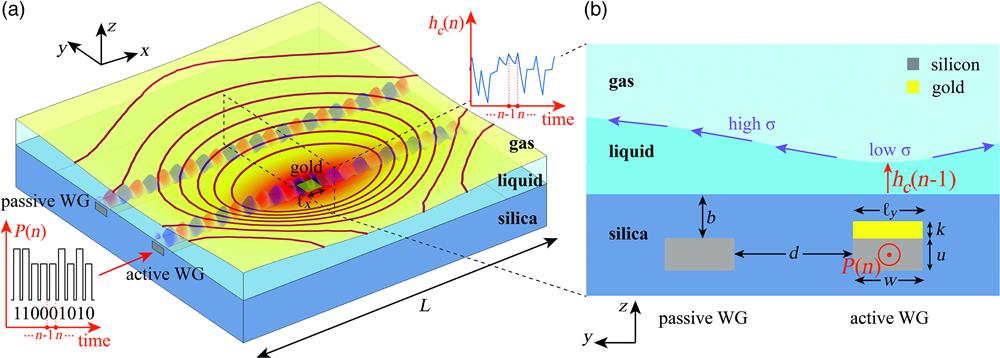
    Fig. 1. Schematic description of the key components in the integrated optofluidic system under study describing the underlying mechanism of the light–liquid interaction and the memory used for RC. (a) 3D perspective presenting a box-shaped liquid cell of length L=10  μm bracketed by vertical silicone walls, and an active Si channel WG on a silica substrate covered with a gold patch of dimensions x×y×k enabling light-induced heating and subsequent heat transport to the gas–liquid interface, which in turn triggers surface tension gradients, represented by blue arrows in (b), leading to the TC effect and liquid film thinning. The latter leads to a self-induced phase change and/or to transmittance change in the single WG setup and also to a nonlocal effect, where the phase in the adjacent passive WG is modified due to liquid deformation. Darker colors on the liquid’s surface in (a) correspond to higher temperature, whereas the dark red lines denote equal height levels. A sequence of high and low optical power pulses correspond to logic “0” and “1,” respectively. The finite relaxation time of the gas–liquid interface allows us to employ it as a short-term memory, where the (n1)th pulse of power P(n1) induces hc(n1) liquid thickness affecting the subsequent nth pulse of power P(n). (b) 2D normal section, consisting of Si channel WGs of width w=500  nm and height u=220  nm buried in depth b=80  nm under silica top surface and hosting a gold patch of thickness k=20 nm and in-plane dimensions x=y=500  nm; the initial liquid depth is h0=500  nm.
    Numerical multiphysics simulation results presenting self-induced phase change in a single active WG covered with a thin liquid film. (a) Deformed gas–liquid interface under 0.1-mW CW light-induced TC effect at time t=20 ms (where t=0 s is the time moment when the optical mode began to propagate) and (b) graphic representation of the internal optical-generated feedback (circular arrow) due to deformation of the gas–liquid interface, allowing us to invoke transient dynamics serving as memory storing the previous optical pulse and using the dynamics to affect the deformed profile and the optical pulse at the next time moments at the same actuation region. The colormap describes electric field magnitude along the x–z plane at time moment t=20 ms; the gold patch resides on the top facet of the WG, and its dimensions along the x-axis are bracketed by the white dashed lines. (c) Electrical field magnitude along the normal section y–z at x=−4.5 μm, x=0 μm, and x=4.5 μm corresponding to left, central, and right columns, respectively, under 0.1 mW incident intensity; first and second rows correspond to mode profiles at initial time t=0 ms and t=20 ms, respectively. (d) The corresponding phase change as a function of different optical powers in the WG due to (e) liquid film thickness change, where hc is liquid thickness above the center of the gold patch. (f) The underlying change of the average temperature of the gold patch, Tc; (g) the corresponding transmittance as a function of time. Key parameters: initial temperature 20°C; wavelength of TM mode is 1550 nm; refractive index of liquid is 1.44 (same as silica substrate); geometric WG parameters are presented in Fig. 1.
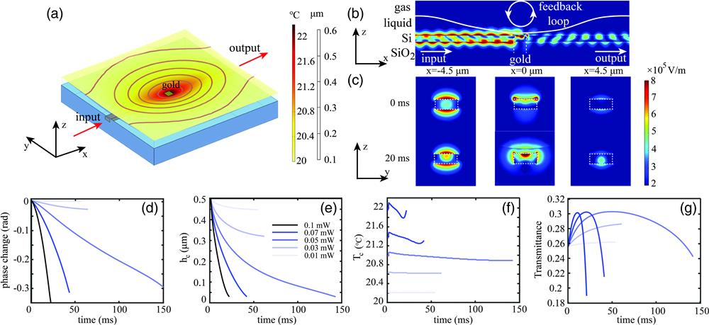
    Fig. 2. Numerical multiphysics simulation results presenting self-induced phase change in a single active WG covered with a thin liquid film. (a) Deformed gas–liquid interface under 0.1-mW CW light-induced TC effect at time t=20  ms (where t=0  s is the time moment when the optical mode began to propagate) and (b) graphic representation of the internal optical-generated feedback (circular arrow) due to deformation of the gas–liquid interface, allowing us to invoke transient dynamics serving as memory storing the previous optical pulse and using the dynamics to affect the deformed profile and the optical pulse at the next time moments at the same actuation region. The colormap describes electric field magnitude along the xz plane at time moment t=20  ms; the gold patch resides on the top facet of the WG, and its dimensions along the x-axis are bracketed by the white dashed lines. (c) Electrical field magnitude along the normal section yz at x=4.5  μm, x=0  μm, and x=4.5  μm corresponding to left, central, and right columns, respectively, under 0.1 mW incident intensity; first and second rows correspond to mode profiles at initial time t=0  ms and t=20  ms, respectively. (d) The corresponding phase change as a function of different optical powers in the WG due to (e) liquid film thickness change, where hc is liquid thickness above the center of the gold patch. (f) The underlying change of the average temperature of the gold patch, Tc; (g) the corresponding transmittance as a function of time. Key parameters: initial temperature 20°C; wavelength of TM mode is 1550 nm; refractive index of liquid is 1.44 (same as silica substrate); geometric WG parameters are presented in Fig. 1.
    Numerical results demonstrating self-induced nonlocal interaction between two adjacent WGs in (a)–(c) the close and (d)–(f) far separation regimes, due to continuous TM mode of wavelength 1550 nm injected to the active WG leading to TC-driven deformation of the liquid film; geometric parameters of WGs and the gold patch are provided in Fig. 1. (a)–(c) Close separation regime with directional coupler geometry of d=0.4 μm and interaction length L=4.7 μm. (a) Temperature field and the geometry of the gas–liquid interface at time t=23 ms under 0.1 mW; (b) top view of the WGs with the gold patch of longitudinal dimension ℓx=0.5 μm and the corresponding optical field at t=23 ms; (c) numerical simulation results of optical intensity change in both WGs as a function of time. (d), (e) Far separation regime presenting three cases of parallel WGs separated by distances d=1,2,3 μm and corresponding gold patches of lateral dimensions ℓy=d+w. (d) Temperature field and the topography of the gas–liquid interface at time t=27 ms under 0.1 mW for the case d=2 μm; (e) side view of the WGs with an elongated gold patch along the transverse direction, ℓy, to facilitate heat transport from the active WG to passive WG and numerical results of two simulations at time 27 ms, where the mode is injected into active or passive WGs, indicating that the gold stripe does not support propagation of surface plasmon polaritons between the WGs. (f) Phase change in the passive WG mode as a function of time, for three different distances from the active WG.
    Fig. 3. Numerical results demonstrating self-induced nonlocal interaction between two adjacent WGs in (a)–(c) the close and (d)–(f) far separation regimes, due to continuous TM mode of wavelength 1550 nm injected to the active WG leading to TC-driven deformation of the liquid film; geometric parameters of WGs and the gold patch are provided in Fig. 1. (a)–(c) Close separation regime with directional coupler geometry of d=0.4  μm and interaction length L=4.7  μm. (a) Temperature field and the geometry of the gas–liquid interface at time t=23  ms under 0.1 mW; (b) top view of the WGs with the gold patch of longitudinal dimension x=0.5  μm and the corresponding optical field at t=23  ms; (c) numerical simulation results of optical intensity change in both WGs as a function of time. (d), (e) Far separation regime presenting three cases of parallel WGs separated by distances d=1,2,3  μm and corresponding gold patches of lateral dimensions y=d+w. (d) Temperature field and the topography of the gas–liquid interface at time t=27  ms under 0.1 mW for the case d=2  μm; (e) side view of the WGs with an elongated gold patch along the transverse direction, y, to facilitate heat transport from the active WG to passive WG and numerical results of two simulations at time 27 ms, where the mode is injected into active or passive WGs, indicating that the gold stripe does not support propagation of surface plasmon polaritons between the WGs. (f) Phase change in the passive WG mode as a function of time, for three different distances from the active WG.
    Numerical simulation results of the self-induced transmittance and reflection effects. (a) The underlying 3D geometric setup of the periodic SiN Bragg WG on silica substrate and (b) the corresponding 2D normal cross section in the x–z plane. Here, a=0.7 μm, b=0.4 μm, c=r=0.2775 μm, k=20 nm; number of ribs without gold patch n=4 and with gold patch m=15 for optimized performance. (c) Colormap of the corresponding power-flow along the WG as a function of time. At successively later time moments, liquid film over the periodic structure becomes increasingly thinner, thus facilitating optical propagation through the periodic structure designed to admit a stop band in the presence of liquid film. (d) Transmittance (black curve) as a function of time presenting also the transmittance values for thin liquid topography presented for the corresponding time moments in (c). The blue curve presents the decreasing function of transmittance for the complementary case of self-induced reflection, where a similar structure increasingly rejects light as liquid thickness approaches zero (see the Supplementary Material for more details as well as the video file showing the corresponding 3D liquid deformation as a function of time) (Video 1, mp4, 6.40 MB [URL: https://doi.org/10.1117/1.AP.4.4.046005.1]).
    Fig. 4. Numerical simulation results of the self-induced transmittance and reflection effects. (a) The underlying 3D geometric setup of the periodic SiN Bragg WG on silica substrate and (b) the corresponding 2D normal cross section in the xz plane. Here, a=0.7  μm, b=0.4  μm, c=r=0.2775  μm, k=20  nm; number of ribs without gold patch n=4 and with gold patch m=15 for optimized performance. (c) Colormap of the corresponding power-flow along the WG as a function of time. At successively later time moments, liquid film over the periodic structure becomes increasingly thinner, thus facilitating optical propagation through the periodic structure designed to admit a stop band in the presence of liquid film. (d) Transmittance (black curve) as a function of time presenting also the transmittance values for thin liquid topography presented for the corresponding time moments in (c). The blue curve presents the decreasing function of transmittance for the complementary case of self-induced reflection, where a similar structure increasingly rejects light as liquid thickness approaches zero (see the Supplementary Material for more details as well as the video file showing the corresponding 3D liquid deformation as a function of time) (Video 1, mp4, 6.40 MB [URL: https://doi.org/10.1117/1.AP.4.4.046005.1]).
    Simulation results presenting RC computing of the XOR task by employing self-induced phase change (nonlinear) and self-induced coupling change (nonlocal) effects. (a) Schematic diagram presenting the MZI circuit with two linear couplers, where the liquid cell introduces self-induced phase change in one of the arms measured by a pair of detectors D1,2, (b) encoding scheme of “0” (“1”), which employs a square wave modulation with actuation period τw of power 2P (P), followed by relaxation period τr, and (c) nonlocal circuit, which employs self-induced coupling change and identical encoding. (d) Test results presenting performance error of the XOR task for delay parameter δ=1 as a function of Pmax and relaxation time τr in nonlinear circuit (a), and colormap (e) performing an identical task with nonlocal circuit (c) demonstrating the enhanced area of vanishing error. (f) Test results of the XOR task with δ=2 using nonlocal circuit (c) showing minimal error ∼11%. (g) Dynamics evolution of the optical signal in detector D1 (blue) and liquid thickness hc (red) due to the actuation signal (green) with τw=25 ms, τr=5 ms, and P=0.033 mW. (h) Folded dynamics of optical intensity in the nonlinear circuit and (i) nonlocal circuit showing enhanced separability of the different regimes.
    Fig. 5. Simulation results presenting RC computing of the XOR task by employing self-induced phase change (nonlinear) and self-induced coupling change (nonlocal) effects. (a) Schematic diagram presenting the MZI circuit with two linear couplers, where the liquid cell introduces self-induced phase change in one of the arms measured by a pair of detectors D1,2, (b) encoding scheme of “0” (“1”), which employs a square wave modulation with actuation period τw of power 2P (P), followed by relaxation period τr, and (c) nonlocal circuit, which employs self-induced coupling change and identical encoding. (d) Test results presenting performance error of the XOR task for delay parameter δ=1 as a function of Pmax and relaxation time τr in nonlinear circuit (a), and colormap (e) performing an identical task with nonlocal circuit (c) demonstrating the enhanced area of vanishing error. (f) Test results of the XOR task with δ=2 using nonlocal circuit (c) showing minimal error 11%. (g) Dynamics evolution of the optical signal in detector D1 (blue) and liquid thickness hc (red) due to the actuation signal (green) with τw=25  ms, τr=5  ms, and P=0.033  mW. (h) Folded dynamics of optical intensity in the nonlinear circuit and (i) nonlocal circuit showing enhanced separability of the different regimes.
    RC of analog task: classification of hand-written “zero” and “one” digits. (a) Sample of 20 images each of size 28×28 pixels, which were used for classification. (b) Detailed “one” image with (c) presenting the encoded signal along a single red horizontal row; the bits of two adjacent rows are injected in parallel into the two input arms of nonlocal [Fig. 5(a)] or nonlinear [Fig. 5(c)] circuits. (d) Classification error of both training and test stages, each employing 12,665 and 2115 images, respectively. The nonlocal circuit with minimal error of 0.14% demonstrates enhanced performance compared to the nonlinear circuit with minimal error of 0.24%. Employing just one arm of the MZI for bits injection, i.e., injecting only one row at a time, increases the classification error for nonlinear circuits to ∼0.55% for similar Pmax values.
    Fig. 6. RC of analog task: classification of hand-written “zero” and “one” digits. (a) Sample of 20 images each of size 28×28  pixels, which were used for classification. (b) Detailed “one” image with (c) presenting the encoded signal along a single red horizontal row; the bits of two adjacent rows are injected in parallel into the two input arms of nonlocal [Fig. 5(a)] or nonlinear [Fig. 5(c)] circuits. (d) Classification error of both training and test stages, each employing 12,665 and 2115 images, respectively. The nonlocal circuit with minimal error of 0.14% demonstrates enhanced performance compared to the nonlinear circuit with minimal error of 0.24%. Employing just one arm of the MZI for bits injection, i.e., injecting only one row at a time, increases the classification error for nonlinear circuits to ∼0.55% for similar Pmax values.
    Chengkuan Gao, Prabhav Gaur, Shimon Rubin, Yeshaiahu Fainman. Thin liquid film as an optical nonlinear-nonlocal medium and memory element in integrated optofluidic reservoir computer[J]. Advanced Photonics, 2022, 4(4): 046005
    Download Citation