• High Power Laser and Particle Beams
  • Vol. 32, Issue 2, 025015 (2020)
Wei Tong1、1、2、2, Hua Li1、1, Peng Fu1、1, Kun Wang1、1、2、2, Ul Hassan Mahmood1、1, and Zhiquan Song1、1、*
Author Affiliations
  • 1Institute of Plasma Physics, Chinese Academy of Sciences, Hefei 230031, China
  • 2Science Island Branch, University of Science and Technology of China, Hefei 230026, China
  • show less
    DOI: 10.11884/HPLPB202032.190280 Cite this Article
    Wei Tong, Hua Li, Peng Fu, Kun Wang, Ul Hassan Mahmood, Zhiquan Song. A parameter optimization method of snubber circuit of thyristor under pulse current working condition[J]. High Power Laser and Particle Beams, 2020, 32(2): 025015 Copy Citation Text show less
    Simplified commutation diagram of quench protection system (QPS)
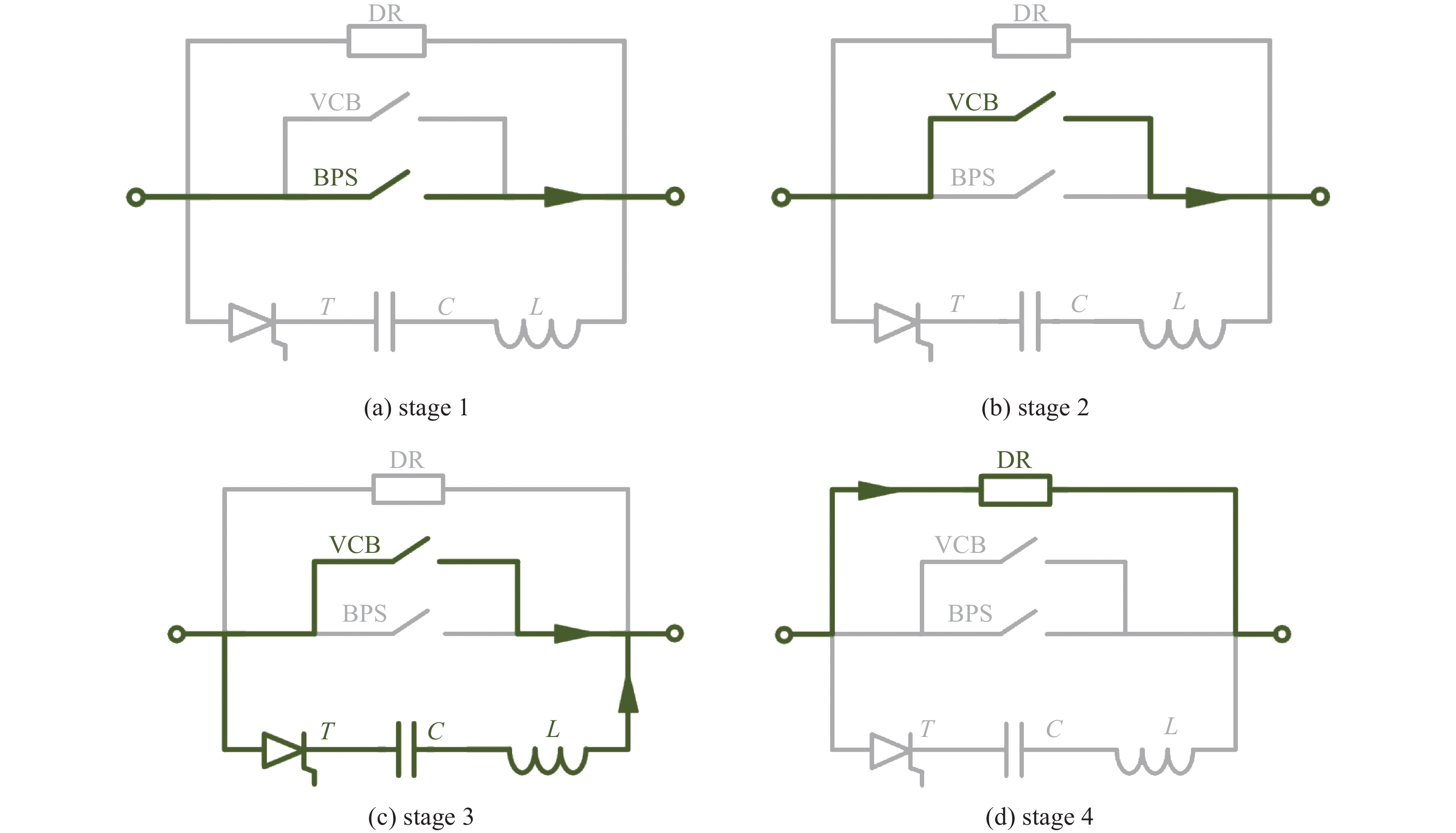
    Fig. 1. Simplified commutation diagram of quench protection system (QPS)
    Exponential function model指数型模型波形图
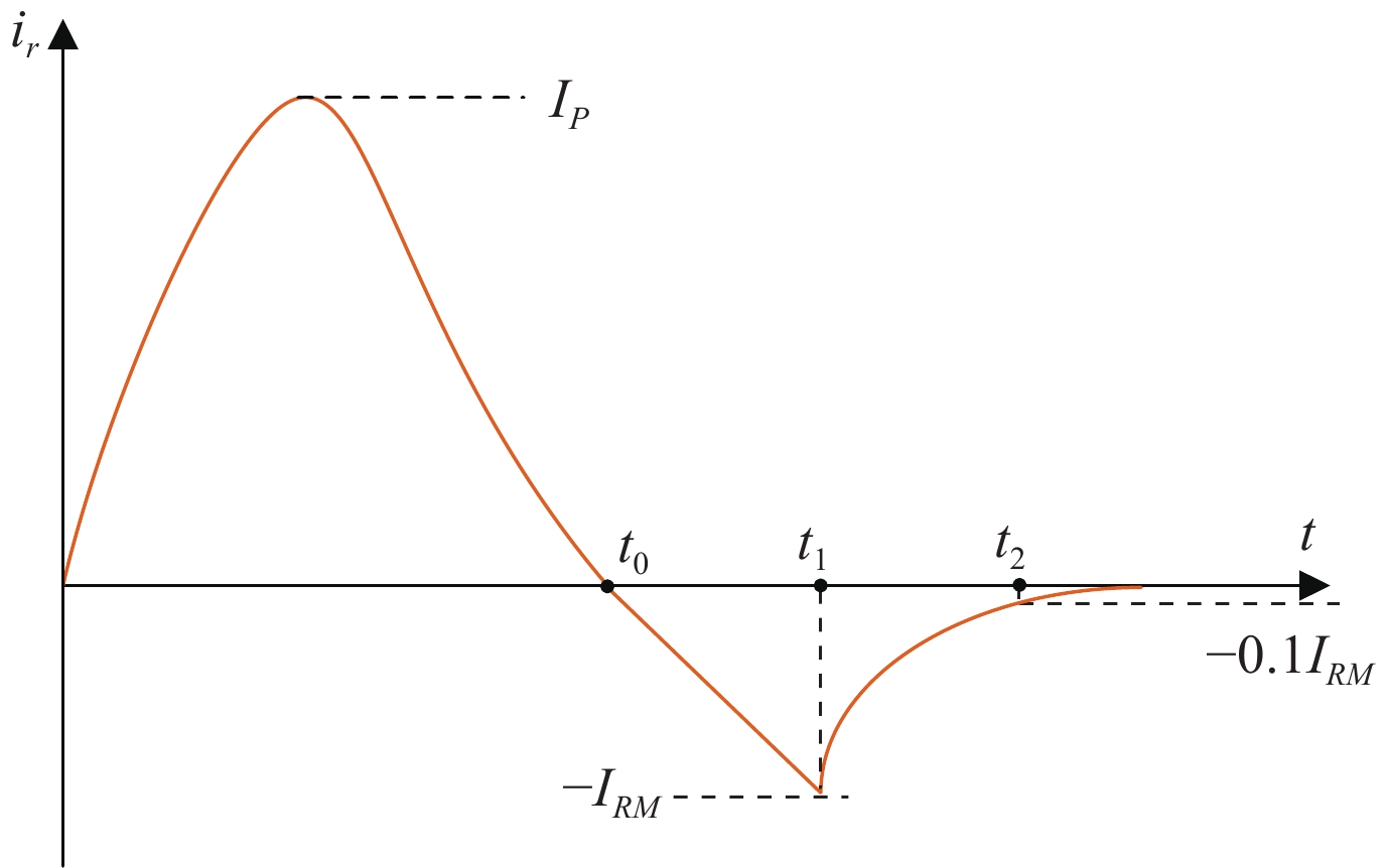
    Fig. 2. Exponential function model指数型模型波形图
    Test circuit for thyristor reverse recovery characteristic脉冲工况下晶闸管测试实验电路图
    Fig. 3. Test circuit for thyristor reverse recovery characteristic脉冲工况下晶闸管测试实验电路图
    Equivalent circuit diagram of snubber circuit during the reverse recovery process
    Fig. 4. Equivalent circuit diagram of snubber circuit during the reverse recovery process
    Peak value of Vdmax under various set of Rs and Cs.
    Fig. 5. Peak value of Vdmax under various set of Rs and Cs.
    Peak value of dVd/dt under various set of Rs and Cs
    Fig. 6. Peak value of dVd/dt under various set of Rs and Cs
    Peak value of dVd/dt as a function of Rs
    Fig. 7. Peak value of dVd/dt as a function of Rs
    Peak value of Vd as a function of Rs and Cs
    Fig. 8. Peak value of Vd as a function of Rs and Cs
    Comparison of reverse recovery current and voltage waveforms
    Fig. 9. Comparison of reverse recovery current and voltage waveforms
    charge voltage/VIp/A IRM/A di/dt/ (A·µs−1) Qrr/µC
    1 0006 62289537.108 057.3
    1 5009 93596750.968 412.8
    2 00013 2501 10076.549 049.2
    2 50016 5601 20697.419 568.7
    3 00019 8801 330121.2210 153.0
    3 50023 1901 402135.9710 505.4
    4 00026 5001 523160.2611 076.2
    4 50029 8101 627179.4411 517.1
    5 00033 1601 738198.9811 962.4
    5 50036 4801 846221.8812 471.5
    6 00039 7901 915238.7612 849.6
    6 50043 0902 014256.9013 244.7
    7 00046 3802 132279.0113 715.9
    7 50049 8802 230298.3714 122.1
    Table 1. Specific characteristics of thyristor during reverse recovery process
    symbolparametervalue
    L/µH external inductance25
    VdRM, VRRM/V max. repetitive peak forward and reverse blocking voltage of chosen thyristor5 200
    dVd/dtcrit/(V·µs-1) critical rate of rise of commutating voltage of chosen thyristor(di/dt=500 A/µs, Tvj=125 ℃) 3 000
    IRM/A peak value of reverse recovery current (di/dt=500 A/µs, Tvj=125 ℃) 1 825.7
    NSthyristor series number2
    Table 2. Design specification of RC snubber circuit for QPS in LSTF
    symbolparametervalue
    RsSnubber Resistance11.3
    Cs/μF Snubber Capacitance0.8
    Vdmax/V Maximum Reverse Recovery Voltage6 210
    (dVd/dt)max/(V·μs−1) Maximum Vd change rate 3 600
    Table 3. The optimum Rs, Cs and corresponding circuit parameters
    optimum parametersPractical parameters
    IRM /A) 1 8151 835
    (di/dt)0/(A·s-1) 309×106307×106
    vdmax/V 6 1686 960
    (dVd/dt)max /(V·µs-1) 3 5986 285
    Table 4. Comparison of electrical parameters
    Wei Tong, Hua Li, Peng Fu, Kun Wang, Ul Hassan Mahmood, Zhiquan Song. A parameter optimization method of snubber circuit of thyristor under pulse current working condition[J]. High Power Laser and Particle Beams, 2020, 32(2): 025015
    Download Citation