
Zhao Chen, Yudong Weng, Junku Liu, Nan Guo, Yaolun Yu, Lin Xiao, "Dual-band perfect absorber for a mid-infrared photodetector based on a dielectric metal metasurface," Photonics Res. 9, 27 (2021)
- Photonics Research
- Vol. 9, Issue 1, 27 (2021)
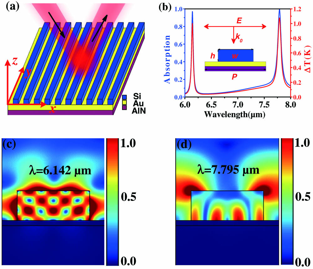
Fig. 1. (a) Schematic of the resonant absorption structure based on dielectric–metal metasurface. (b) Theoretical absorption spectrum (blue line) and normalized average temperature increasing of the sensitive material upper surface, Δ T | E | λ = 6.142 μm λ = 7.795 μm
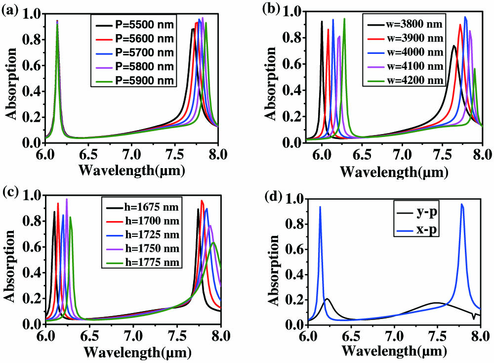
Fig. 2. Optical properties of the metastructure absorber. The graphs show the spectra of absorption with different (a) period P w h E
Fig. 3. Temporal temperature distributions for (a) different substrate materials with the same incident flux I 0 = 10 3 W / cm 2 I 0 = 1.0 W / cm 2
Fig. 4. Temporal temperature distributions for different (a) pulse time t h htc t = 1.0 ms I 0 = 1.0 W / cm 2
Fig. 5. Temporal temperature distributions for 100 × I 0 = 1.0 W / cm 2 t = 0.4 ms
Fig. 6. Schematic of a single metasurface element used for both the electromagnetic and heat transfer simulations and their associated boundary conditions.
Fig. 7. (a), (b) | H | Q abs λ = 6.142 μm λ = 7.795 μm
Fig. 8. (a) Absorption spectrum. (b) Temporal temperature distributions under continuous wave and pulsed wave illumination with incident flux I 0 = 1 W / cm 2 ( t ) = 1 0 < t ≤ 0.1 ms ( t ) = 0 P = 5700 nm w = 4000 nm
Fig. 9. (a) Absorption spectra for different incident angle α | E | | H | Q abs λ = 6.865 μm
Fig. 10. Temporal temperature distributions under continuous wave and pulsed wave illumination for different substrate materials (a) Si with I 0 = 10 3 W / cm 2 SiO 2 I 0 = 15 W / cm 2
Fig. 11. Simulated temporal temperature distributions after excitation with a fs-pulse.
|
Table 1. Thermal Parameters of the Materials Used in Our Metastructures


Set citation alerts for the article
Please enter your email address

© Copyright 2018-2021 | Chinese Laser Press. All Rights Reserved 沪ICP备15018463号-20