• Chinese Physics B
  • Vol. 29, Issue 8, (2020)
Qilang Wang1, Yunyu Chen2, Adili Aiyiti1, Minrui Zheng3, Nianbei Li4、†, and Xiangfan Xu1
Author Affiliations
  • 1Center for Phononics and Thermal Energy Science, China-EU Joint Center for Nanophononics, School of Physics Science and Engineering, Tongji University, Shanghai 200092, China
  • 2The First Affiliated Hospital of Wenzhou Medical University, Wenzhou 35000, China
  • 3Department of Electrical and Computer Engineering, Faculty of Engineering, National University of Singapore, 4 Engineering Drive , Singapore11758
  • 4Institute of Systems Science and Department of Physics, College of Information Science and Engineering, Huaqiao University, Xiamen 361021, China
  • show less
    DOI: 10.1088/1674-1056/ab90f0 Cite this Article
    Qilang Wang, Yunyu Chen, Adili Aiyiti, Minrui Zheng, Nianbei Li, Xiangfan Xu. Scaling behavior of thermal conductivity in single-crystalline α-Fe2O3 nanowires[J]. Chinese Physics B, 2020, 29(8): Copy Citation Text show less
    Sample characterization. (a) TEM image of the single α-Fe2O3 nanowire. (b) HRTEM image and FFT ED pattern revealing single crystal structure of the nanowire. (c) XRD patterns and (d) Raman spectrum of the α-Fe2O3 nanowires.
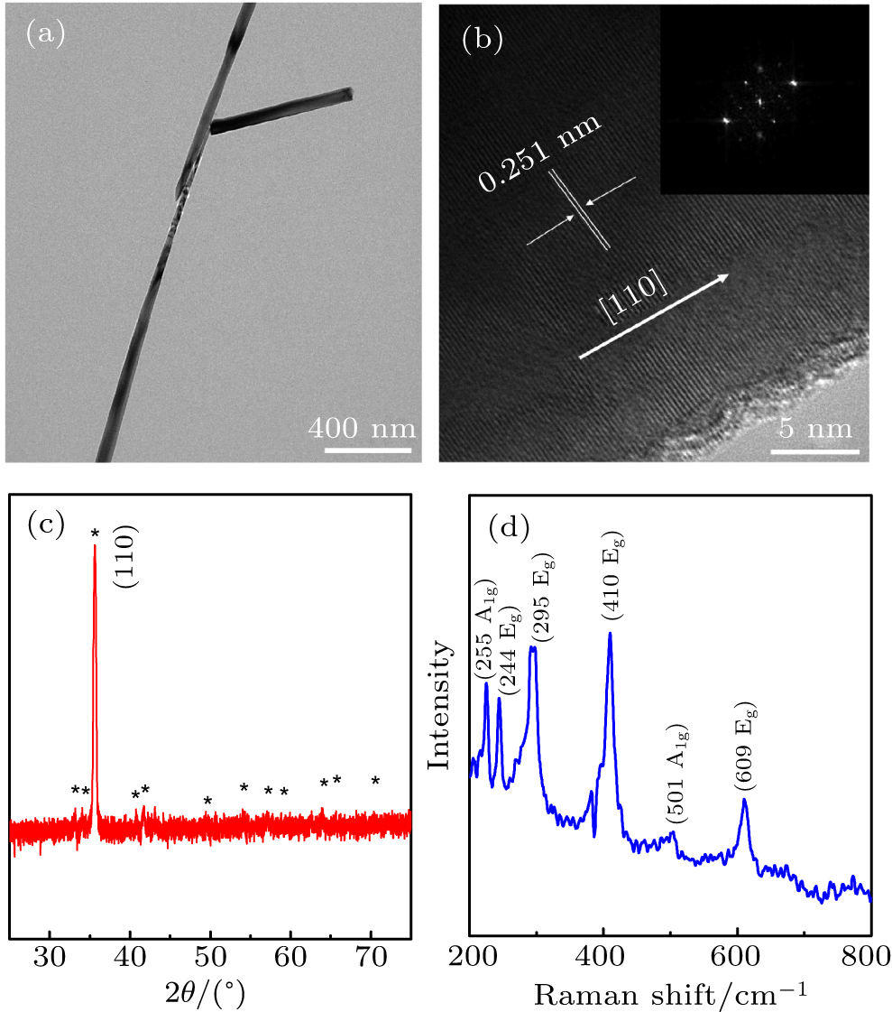
    Fig. 1. Sample characterization. (a) TEM image of the single α-Fe2O3 nanowire. (b) HRTEM image and FFT ED pattern revealing single crystal structure of the nanowire. (c) XRD patterns and (d) Raman spectrum of the α-Fe2O3 nanowires.
    Suspended sample preparation. (a) SEM image of the grass-like grown α-Fe2O3 nanowire arrays on the Fe foil. (b) SEM image of some free lying individual α-Fe2O3 nanowires on the SiO2/Si substrate. (c) Image of the micromanipulator miBotTM armed with a sharp tungsten tip. (d) SEM image of the as-prepared suspended α-Fe2O3 nanowire whose two ends are fastened to the electrodes of the microdevice by EBID.
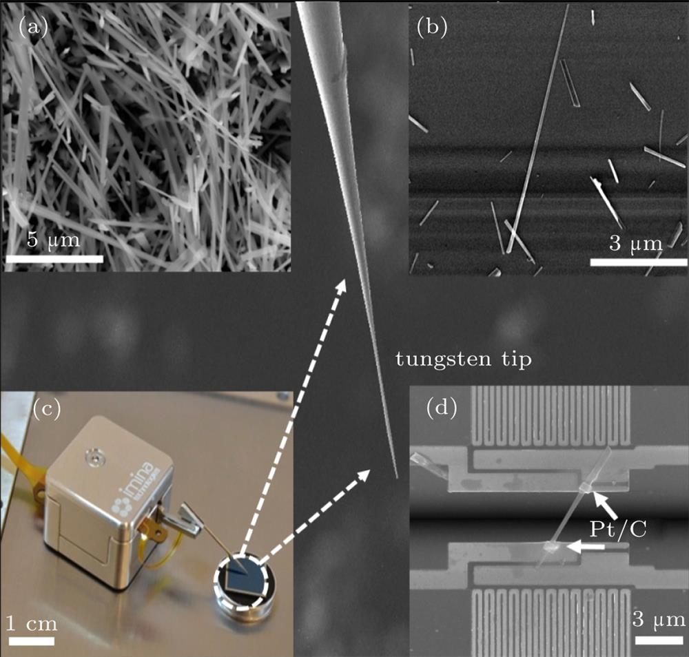
    Fig. 2. Suspended sample preparation. (a) SEM image of the grass-like grown α-Fe2O3 nanowire arrays on the Fe foil. (b) SEM image of some free lying individual α-Fe2O3 nanowires on the SiO2/Si substrate. (c) Image of the micromanipulator miBotTM armed with a sharp tungsten tip. (d) SEM image of the as-prepared suspended α-Fe2O3 nanowire whose two ends are fastened to the electrodes of the microdevice by EBID.
    (a) The schematic of the EBID process. (b) H vs. time shows the Pt/C deposition rate (20 nm/min). The red dash line is the best linear fitting to the data. (c) The typical cumulative thermal resistance (Ri) was obtained when the focused electron beam was scanning along the individual nanowires. The upper inset is the schematic of the electron beam self-heating technique and the lower shows the SEM image of the scanned nanowire. (d) Influence of EBID time/hight on the thermal contact of the nanowire shown in the lower inset of (c). The red balls and blue diamonds denote the thermal conductance and conductivity measured with the thermal bridge method at T = 300 K for the nanowire, respectively. The blue stars are the intrinsic thermal conductivity derived from the electron beam self-heating technique for the specific nanowire at T = 300 K. (e) The measured thermal resistance R (black diamonds) and the derived thermal contact resistance Rc (red balls) of the nanowire vs. time. (f) Rc/R vs. time. All the solid curves in (d)–(f) are a guide to the eyes.
    Fig. 3. (a) The schematic of the EBID process. (b) H vs. time shows the Pt/C deposition rate (20 nm/min). The red dash line is the best linear fitting to the data. (c) The typical cumulative thermal resistance (Ri) was obtained when the focused electron beam was scanning along the individual nanowires. The upper inset is the schematic of the electron beam self-heating technique and the lower shows the SEM image of the scanned nanowire. (d) Influence of EBID time/hight on the thermal contact of the nanowire shown in the lower inset of (c). The red balls and blue diamonds denote the thermal conductance and conductivity measured with the thermal bridge method at T = 300 K for the nanowire, respectively. The blue stars are the intrinsic thermal conductivity derived from the electron beam self-heating technique for the specific nanowire at T = 300 K. (e) The measured thermal resistance R (black diamonds) and the derived thermal contact resistance Rc (red balls) of the nanowire vs. time. (f) Rc/R vs. time. All the solid curves in (d)–(f) are a guide to the eyes.
    Temperature and size dependent thermal conductivity of the individual nanowires. (a) G vs. T. The red dash line shows the T−1 dependency. (b) L/κ vs. d at T = 300 K, the green dashed line is a guide to the eyes.
    Fig. 4. Temperature and size dependent thermal conductivity of the individual nanowires. (a) G vs. T. The red dash line shows the T−1 dependency. (b) L/κ vs. d at T = 300 K, the green dashed line is a guide to the eyes.
    Samples1234567891011
    L/μm9.886.3110.474.845.806.637.0116.2415.7820.7311.64
    d/nm420310241256370318300448370661180
    κ/W⋅m−1⋅K−17.316.2111.9010.836.318.8410.1910.8612.647.8637.72
    Table 1. Details of the measured individual nanowires.
    Qilang Wang, Yunyu Chen, Adili Aiyiti, Minrui Zheng, Nianbei Li, Xiangfan Xu. Scaling behavior of thermal conductivity in single-crystalline α-Fe2O3 nanowires[J]. Chinese Physics B, 2020, 29(8):
    Download Citation