
Hideo Isshiki, Fangli Jing, Takuya Sato, Takayuki Nakajima, Tadamasa Kimura, "Rare earth silicates as gain media for silicon photonics [Invited]," Photonics Res. 2, A45 (2014)
- Photonics Research
- Vol. 2, Issue 3, A45 (2014)

Fig. 1. PL spectra of Er x Y 2 − x SiO 5
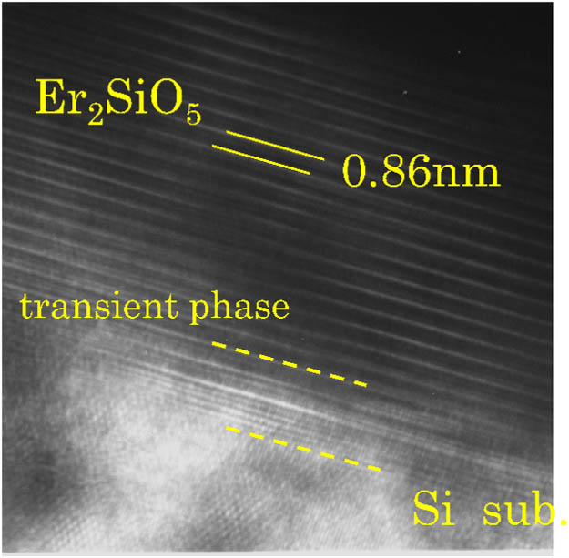
Fig. 2. TEM image of highly oriented Er 2 SiO 5
Fig. 4. XRD patterns of Er x Y 2 − x SiO 5 Er x Yb y Y 2 − x − y SiO 5 x = 0.33 y = 0.33
Fig. 5. XRD patterns of Er x Y 2 − x SiO 5
Fig. 6. PL emission of Er x Y 2 − x SiO 5 Er x Y b y Y 2 − x − y SiO 5 I 4 13 / 2 → I 4 15 / 2 Er 3 +
Fig. 7. PL intensity ratio of Er x Yb y Y 2 − x − y SiO 5 Er x Y 2 − x SiO 5
Fig. 8. 1.53 μm emission decay rate as a function of the Er concentration. The solid lines show the fitting curves by Eq. (5 ).
Fig. 9. Schematic diagram of the spherical grain model. Density plots show distribution of the excited Er ions at the steady state.
Fig. 10. CUC emission spectra of the sol–gel sample. The energy diagram and CUC energy transfer process are also shown.
Fig. 11. CUC process modeling of the Er x Y 2 − x SiO 5
Fig. 12. CUC emission intensity as a function of excitation power. The solid line is a calculation result using the rate equation [Eq. (6 )] with C up = 1 × 10 − 17 cm 3 s − 1
Fig. 13. Summary plots of the CUC coefficients as a function of Er concentration for various host materials [13,29,3436" target="_self" style="display: inline;">–36 ]. The dashed line shows the linear dependence expected from the Förster energy transfer.
Fig. 14. Schematic diagram of the waveguide with buried Si guide layer.
Fig. 15. Top views of the Er x Y 2 − x SiO 5 x = 0.45
Fig. 16. Decay coefficient as a function of Er concentration. The solid line is the linear approximation of a series of the sol–gel samples.
Fig. 17. Schematic diagram of Er x Y 2 − x SiO 5
Fig. 18. Top views of the Si PhC–S Er 0.4 Y 1.6 SiO 5
Fig. 19. (a) PL spectra and the edge emission intensity versus (b) exposed length from the Si PhC–S Er 0.4 Y 1.6 SiO 5
Fig. 20. Gain characteristics of Si PhC–S Er 0.4 Y 1.6 SiO 5
| ||||||||||||||||||||||||||||||||||||||||
Table 1. Parameters Used in the Rate Equation Modeling of the


Set citation alerts for the article
Please enter your email address

© Copyright 2018-2021 | Chinese Laser Press. All Rights Reserved 沪ICP备15018463号-20