
Xu Liu, Shengjun Zhou, "Progress on photovoltaic AlGaN photodiodes for solar-blind ultraviolet photodetection," Chin. Opt. Lett. 20, 112501 (2022)
- Chinese Optics Letters
- Vol. 20, Issue 11, 112501 (2022)
Abstract
1. Introduction
Ultraviolet (UV) light accounts for 10% of the total solar spectrum. Based on the wavelength of UV light, the whole radiation region is divided into the four subregions: UVA (400–320 nm), UVB (320–280 nm), UVC (280–100 nm), and extreme UV (EUV) (120–10 nm)[
III-nitride semiconductors, including GaN, AlN, InN, and their ternary (AlGaN, InGaN) and quaternary alloys (AlGaInN), exhibit superior properties, such as a wide energy bandgap, large thermal conductivity, high carrier mobility, strong anti-radiation ability, and good chemical stability[
According to the operation mode, solar-blind ultraviolet photodetectors (SBPDs) are generally divided into photoconductive SBPDs and photovoltaic SBPDs. Photoconductive SBPDs have been investigated in the past several decades. Their photodetection behavior is based on the fact that the electrical conductivity of SBPDs will change when exposed to the radiation of solar-blind UV light. Photoconductive SBPDs are fit for mass production. However, they also suffer from several fatal drawbacks, including slow response speed, low-energy photon response, and severe temperature dependence. Photovoltaic SBPDs are those photodetectors whose work mechanism is based on the photovoltaic effect. The electric field resulting from the photovoltaic effect at the interfaces can facilitate the separation and transport of photogenerated carriers, thereby resulting in enhanced responsivity and response speed of photovoltaic SBPDs. There are several configurations of photovoltaic photodiodes used for solar-blind UV photodetection, including p-n/p-i-n, Schottky barrier, metal-semiconductor-metal (MSM), and avalanche photodiodes (APDs). In recent years, photovoltaic AlGaN photodiodes have been rapidly developed, which is important for the development of high-performance SBPDs.
Sign up for Chinese Optics Letters TOC. Get the latest issue of Chinese Optics Letters delivered right to you!Sign up now
In this review, we summarize recent development of photovoltaic AlGaN SBPDs. First, we focus on the AlGaN epilayers and low-defect AlN/sapphire template. Then, we discuss several types of photovoltaic AlGaN SBPDs, including device configurations, performance improvement methods, and physical mechanisms. Moreover, the advances in photovoltaic AlGaN SBPDs are reviewed to better understand solar-blind UV photodetection technology for versatile applications.
2. AlGaN Materials
The crystalline quality of AlGaN alloys exerts a strong influence on the detection performance of AlGaN SBPDs. This section is focused on the fabrication methods of AlGaN epitaxial films and their corresponding template techniques.
2.1. AlGaN epitaxial films
Three methods are mainly used to grow the AlGaN absorption layers, including liquid phase epitaxy (LPE), molecular beam epitaxy (MBE), and vapor phase epitaxy (VPE)[
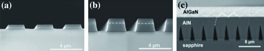
![]()
Figure 1.Cross-section SEM images of (a) stripe-shaped PSS, (b) AlN/PSS template, and (c) AlGaN epitaxial film grown on AlN/PSS template. Reproduced with permission[
2.2. Van der Waals epitaxy of AlN template
Van der Waals epitaxy (vdWE) is quite different from conventional epitaxy owing to the noncovalent bond between the epitaxial material and the substrate at the interface. Although the orientation relationship of the epitaxial material is consistent with the substrate, lattice match is not important for vdWE, which is called incommensurate epitaxy; the in-plane lattice parameters of the three-dimensional (3D) materials will be very close to the bulk value, resulting in no excessive strain and dislocation originating from the lattice mismatch. Recently, AlN vdWE technology has drawn much scientific interest[
![]()
Figure 2.(a) Schematic diagram of the DUV LED grown on AlN/Gr/NPSS. (b) EL spectra of the DUV-LEDs with and without the Gr interlayer. Cross-sectional SEM images of AlN films on NPSS (c) without and (d) with the Gr interlayer. AlN has realized complete coalescence below a thickness of 1 µm in (d), which is less than half of the thickness (about 2.4 µm) on bare NPSS in (c). Reproduced with permission[
2.3. Bulk AlN template
Bulk AlN is anticipated to act as a promising transparent substrate material for nitride devices because of the high thermal conductivity of up to 2.85 W/(cm K). The crystal quality of AlGaN grown on a bulk AlN substrate is intrinsically expected to be good because they both have the same crystallographic symmetry of wurtzite. Therefore, the use of the bulk AlN substrate during the photodetectors manufacturing is worth investigation[
2.4. AlN/sapphire template
Due to large lattice mismatch between the AlGaN and sapphire substrate, there are a vast number of dislocations and point defects existing in the AlGaN epilayers deposited on sapphire substrates. The high-density defects in AlGaN usually act as the non-radiative recombination centers, the carrier scattering centers, and the leakage current channels. The growth of high-quality AlGaN film is the key factor for obtaining high performance SBPDs[
| Template | Thickness (μm) | Nucleation Layer | Defect Density | Highlights | Ref. |
|---|---|---|---|---|---|
| AlN/MPSS | 10.6 | LT-AlN | Total: | 1. PALE-induced | [ |
| S: | 2. These voids facilitate the defect termination and strain release in the AlN epilayer. | ||||
| E: | |||||
| AlN/FSS | 6 | LT-AlN | TD: | 1. The nanoscale ELOG is achieved on the AlN rods/FSS template. | [ |
| S: | 2. The advantage of the nanoscale ELOG is that even the dislocations in the center of the rod do not have a long distance to bend into the voids between the rods. | ||||
| E: None | 3. TDs bend at slight angles due to the nano-scaled air gaps and the rod diameters by nano-ELOG. | ||||
| AlN/MPSS | 2.54 | – | Total: | 1. The effect of PSS on reducing defect density is investigated. | [ |
| EP: | 2. AlN layers with gradient V/III ratio and period AlN superlattice layers (SLs) are introduced into the AlN epilayer to reduce defect density. | ||||
| 3. The behaviors of defect termination are exhibited quantitatively. | |||||
| AlN/NPSS | 3.25 | LT-AlN | TD: | The intrinsic mechanism of bending dislocations by employing AlN SLs with period high/low V/III ratio is revealed in Fig. | [ |
| AlN/FSS | 2 | Sputtered AlN LT-AlN | EP: | 1. The effect of AlN NL thickness on optical transmittance, strain state, surface morphology, and TD density of AlN epilayer is investigated. | [ |
| 2. The AlN epilayer with O-doped sputtered AlN NL has the highest optical transmittance. | |||||
| 3. The AlN epilayer with undoped sputtered AlN NL has the smoothest surface morphology and lowest TD density. | |||||
| AlN/MPSS | 8–10 | Sputtered AlN | S: | 1. Misaligned AlN growth could be overcome by selecting an appropriate growth temperature. | [ |
| E: | 2. Optimizing the PSS geometries is important for rapid coalescence of the AlN epilayer. In this paper, the grown AlN deviating from the c-axis on sapphire near r-plane sidewalls has less influence on the coalescence of AlN grown from the c-axis-oriented sapphire plane, compared to near n-plane sidewalls. | ||||
| AlN/NPSS | 1 | Sputtered AlN | TD: | 1. The growth temperature can exert a strong impact on the crystalline quality of AlN epitaxial films by influencing the diffusion length of adatoms and lateral growth rate. | [ |
| 2. The flat AlN films are realized on AlN/NPSS with a total coalescence at a growth temperature of 1300°C. | |||||
| AlN/FSS | 85 | – | – | 1. Self-separation of AlN epitaxial film is achieved by the formation of voids at the AlN/sapphire interface during the HVPE growth at 1450°C. | [ |
| 2. Voids are formed by decomposition of sapphire during the HVPE of the AlN epilayer, and their size is dominated by the heating time. |
Table 1. Summary of the Reported AlN/Sapphire Template
Bulk AlN substrates could be good candidates to achieve high-responsivity SBPD due to small lattice mismatch with the epitaxial layers and low dislocation density below
Another method is to take the advantage of the NL[
High temperature annealing (HTA) can reduce dislocation densities by relaxing tensile stress, rearranging the AlN lattice, and facilitating generation of a new interface that has little influence on the lattice constant above/below this interface[
Nucleation conditions of NLs are crucial for acquisition of low-defect-density AlN epitaxial films[
![]()
Figure 3.AFM images of the NLs deposited at (a) 950°C, (b) 1050°C, and (c) 1150°C after being recrystallized at 1250°C. AFM images of AlN epitaxial films on NLs deposited at (d) 850°C, (e) 950°C, (f) 1050°C, (g) 1150°C, and (h) 1250°C. Reproduced with permission[
2.5. p-doping of AlGaN
The p-doping of high-Al-content AlGaN alloys is still considered quite challenging after a few years of development. Achieving satisfactory p-doping AlGaN epilayers in the device level has turned out to be difficult. Many methods are developed to improve the low conductivity or poor contacts of p-AlGaN. For example, a standard solution is that a 10–50 nm p-AlGaN thin layer is generally grown on the top of the p-AlGaN cladding layer in UV LEDs; although the strong absorption of the thin p-AlGaN layer at the emission wavelengths is not avoided, it is still an effective way to realize a reasonably good contact, thereby ensuring stabilized hole injection efficiency into the active region of UV LEDs.
Generally, Mg, Zn, and Be can all be used for p-type doping. The corresponding activation energy (AE) of the Mg, Zn, and Be in GaN are 60, 160, and 370 meV[
Chen et al. reported a type of indium-surfactant-assisted delta doping method for high hole concentration in Mg-doped
2.6. Methods for defect annihilation
The AlN epilayer grown on AlN/PSS is dominated by the ELOG[
![]()
Figure 4.Cross-section TEM images of AlN/FSS without AlN SL in the (a) g = (0002) direction and (b) g =
![]()
Figure 5.(a) Illustration of samples with four types of distinct AlN layer structures. (b) Dislocation density of samples A–D. (c) FWHM and individual rocking curves of samples A–D. (d) Schematic illustration of the growth mechanism and dislocation annihilation for sample C. Reproduced with permission[
We introduced voids into the AlN epilayers on FSS to realize similar defect annihilation in AlN/PSS, as shown in Fig. 6[
![]()
Figure 6.Cross-section TEM images of (a) AlN/FSS and (b) AlN/NPSS in the g =
3. Photovoltaic AlGaN Photodiode SBPDs
Numerous types of photovoltaic photodiodes, including Schottky barrier, MSM, p-n/p-i-n junction, and APDs, have been developed for SBPDs. In this section, we will review the current photovoltaic AlGaN photodiode SBPDs reported in recent years. Several reported photovoltaic AlGaN photodiode SBPDs are summarized in Table 2.
| Absorption Layer | Device | Wavelength (nm) | EQE | Ref. | ||||
|---|---|---|---|---|---|---|---|---|
| Schottky | 90 | 274 | – | 42% | [ | |||
| AlGaN/GaN | Schottky | 44 | 274 | – | – | 21% | [ | |
| Schottky | 530 | 229 | – | – | [ | |||
| Schottky | 41 | 260 | – | 20% | [ | |||
| AlGaN MQWs | p-n | 100 | 250 | – | – | 50% | [ | |
| p-i-n | 79 | 280 | – | 35% | [ | |||
| p-i-n | 110 | 283 | – | 43% | [ | |||
| p-i-n | 62 | 247 | – | 30% | [ | |||
| p-i-n | 136 | 282 | – | – | 72% | [ | ||
| p-i-n | 93 | 280 | – | 42% | [ | |||
| p-i-n | 211 | 289 | – | 92% | [ | |||
| MSM | 140 | 272 | – | – | 64% | [ | ||
| MSM | – | 285 | – | – | – | [ | ||
| MSM | 2750 | 250 | – | – | – | [ | ||
| AlGaN/Al NPs | MSM | 288 | 288 | – | – | – | [ | |
| APD | 79.8 | 270 | – | 37% | [ | |||
| APD | 132 | 281 | – | 58.2% | [ | |||
| APD | 98 | 262 | – | 46% | [ | |||
| APD | 150 | 280 | – | 50% | [ | |||
| APD | – | 275 | – | 98.5% | [ | |||
| AlGaN/GaN | APD | – | 275 | – | – | [ |
Table 2. Summary of Performance Parameters on the Reported AlGaN SBPDs
3.1. Parameters
The simplest configuration of an AlGaN photodiode SBPD includes an AlGaN absorption layer, metal electrodes, and external circuitry used to output electrical signals. The AlGaN absorption layer can be fabricated in various configurations, including wafers, thin films, or even nanostructures. Each of these configurations lends different properties to the fabricated photodetector that helps in enhancing one particular figure-of-merit or another. To characterize any device on the basis of its performance, one requires certain parameters[
3.2. Schottky barrier photodiodes
A typical Schottky barrier SBPD is made up of a metal contact layer and a semiconductor absorption layer. The metal/semiconductor junction exhibits rectifying behavior originated from the electrostatic barrier induced by different work functions of the metal and semiconductor. This electrostatic barrier is also called the Schottky barrier. The SBPDs based on Schottky barrier photodiodes exhibit many advantages, including low dark current, short response time, high QE, high responsivity, and possible zero-bias operations. Nevertheless, the incident light needs to penetrate the metal electrode to interact with the semiconductor so that the metal electrode layer needs to be fabricated into a very thin semitransparent layer, whose absorption coefficient is too high to limit further application of the Schottky barrier photodiodes structure in SBPDs.
Biyikli et al. reported a type of
3.3. MSM
AlGaN MSM photodetectors basically consist of a lightly-doped/undoped AlGaN absorption layer and two metal electrodes deposited on the AlGaN surface to form back-to-back Schottky barrier junctions[
In general, MSM SBPD structures include two metal electrodes with back-to-back Schottky contact. The ideal MSM SBPDs with Schottky contact are not expected to exhibit a photoconductive gain, and the responsivity should not change with the applied bias. However, most of the present AlGaN-based MSM SBPDs exhibit high photoconductive gain and responsivity[
In 2012, Xie et al. reported a kind of
Averine et al. fabricated a kind of
Brendel et al. investigated the influence of absorption layer thickness on the photodetection performance of top and bottom-illuminated
Recently, photonic crystals have been widely applied in fabricating SBPDs. Photonic crystals can be applied for reflective modulation of light by generating photonic bandgaps. When the electromagnetic wave propagates in the optical structure with periodic refractive index variation, the photonic bandgap will be formed to suppress the light propagation in corresponding bands due to the existence of Bragg scattering[
![]()
Figure 7.(a) Schematic diagram of AlGaN-heterostructure MSM SBPD. (b) Responsivity of the MSM SBPD with and without photonic crystals. (c) Reflectivity and transmissivity of the AlGaN MSM SBPD with and without photonic crystals. (d) I-V characteristics of AlGaN MSM SBPD. Reproduced with permission[
![]()
Figure 8.(a) Device structure of the AlGaN MQWs SBPD. (b) I-V characteristic of Al0.64Ga0.36N/Al0.34Ga0.66N SBPD in the dark. (c) Responsivity spectrum of AlGaN MQWs SBPD at -0.5 V. Reproduced with permission[
![]()
Figure 9.Schematic diagrams of (a) Al0.15Ga0.85N/Al0.15Ga0.85N SAM-APD SBPD and (b) dual-periodic DBR. (c) Reflectivity of single- and dual-periodic DBR. (d) Responsivity of the SAM-APD SBPDs with single-/dual-periodic and without DBR at 10 V reverse bias. The single-periodic DBR is composed of 25 pairs of AlN/Al0.55Ga0.45N (A/B). Reproduced with permission[
3.4. p-n and p-i-n
AlGaN p-n junction photodiodes are typical photovoltaic photodiodes that are geometrically made up of a piece of p-AlGaN and a piece of n-AlGaN. Therefore, when operating at zero bias, the depletion region is spontaneously formed at the interface of two semiconductors, and a built-in electric field is concomitantly created. Consequently, an energy barrier is formed near the interface to prevent charge carriers freely transferring across the junction because of the discontinuity in allowed energy states of the two semiconductors at an equilibrium state. Therefore, p-n photodiodes normally exhibit rectifying behavior, which indicates an asymmetric I-V characteristic in the darkness. When the AlGaN p-n photodetectors are placed in the solar-blind illumination, the photons whose energy is higher than the bandgap of AlGaN are absorbed by the AlGaN layer, thereby creating the photogenerated electron–hole pairs on both sides of the junction. Due to the built-in electric field in the depletion region, only the minority carriers on both sides of the junctions can traverse across the depletion region. AlGaN p-n SBPDs have many advantages, including a low working bias, high input impedance, high working frequency, and integration capability that is useful for manufacturing technologies and semiconductor planar processes[
Muhtadi et al. reported a type of high-speed solar-blind AlGaN p-n junction photodetector integrated with high-Al-content AlGaN MQWs, as shown in Fig. 8(a)[
Unlike the p-n junctions, the width of the depletion region in the p-i-n junctions is primarily determined by the thickness of the intrinsic layer. Although concurrently increasing the transit time of photogenerated carriers and reducing the response speed of the photodetectors, a thick intrinsic layer can ensure sufficient light absorption, thereby improving the EQE of the photodetectors. That will facilitate reducing the junction capacitance and the RC-time constant. Hence, it is necessary to compromise the design according to demands of real applications[
In 1999, Parish et al. reported a AlGaN-based p-i-n SBPD with a cut-off wavelength of 285 nm. The measured dark current density was as low as
Then, Tut et al. reported a type of AlGaN p-i-n SBPDs with high breakdown voltage and detectivity via using MOCVD[
Researchers at the Fraunhofer Institute reported AlGaN-based p-i-n SBPDs with different active regions[
Inserting MQWs into the depletion region of p-i-n SBPDs can also facilitate improvement of performance[
3.5. Avalanche photodiodes
The APD is a type of photodiode that uses the avalanche production of carriers at a high reverse bias[
The reported APDs involve the various structures discussed above, including Schottky barrier, p-n, and p-i-n structures[
In 2005, McClintock et al. observed avalanche multiplication in AlGaN p-i-n SBPDs[
Then, Sun et al. reported a type of AlGaN APD SBPD with high multiplication gain[
The AlGaN heterostructure is receiving increasing attention for its excellent properties on APD SBPDs[
Employing distributed Bragg reflectors (DBRs) can also improve the gain of AlGaN APD SBPDs[
3.6. Phototransistor
Another important device structure for photodetection is phototransistors due to the possibility of controlling the channel current by gate bias. By changing the gate bias (
In 2018, Armstrong et al. observed solar-blind photodetection induced by defects in
Zhang et al. reported a high-performance UV phototransistor (UVPT) based on the AlGaN/GaN HEMT with a record high peak responsivity[
Subsequently, Yang et al. investigated the temperature dependence of UV photodetection behavior in AlGaN/GaN UVPT under 265 nm illumination[
4. Enhanced Techniques of AlGaN SBPDs
In previous sections, we introduced the research achievements of AlGaN epitaxial films, AlN/sapphire templates, and various kinds of photovoltaic AlGaN-based SBPDs with various configurations. In this part, we will review the recent enhanced techniques of AlGaN SBPDs. Several reported enhanced techniques for photovoltaic AlGaN photodiode SBPDs are summarized in Table 3.
| Absorption Layer | Enhanced Technique | Wavelength (nm) | Ref. | ||
|---|---|---|---|---|---|
| Polarization | 280 | [ | |||
| Polarization | 3.1 | 280 | [ | ||
| Polarization | 12.5 | 266 | [ | ||
| AlxGa1−xN | Polarization | 0.204 | 274 | [ | |
| AlN | Surface modification | 200 | [ | ||
| Surface modification | 7.6 | 250 | [ | ||
| Surface modification | 2.75 | 250 | [ | ||
| Surface modification | 260 | [ | |||
| AlGaN | LSPR | 0.288 | 288 | [ | |
| LSPR | 2.34 | 269 | [ | ||
| LSPR | 0.3 | 265 | [ | ||
| LSPR | 2.7 | 280 | [ | ||
| Ru/AlGaN | PCE | – | 0.0488 | 254 | [ |
| Pt/AlGaN | PCE | – | 0.045 | 254 | [ |
Table 3. Summary of Performance Parameters on the Enhanced Techniques of Reported AlGaN SBPDs
4.1. Polarization effect
AlGaN alloys possess strong spontaneous and piezoelectric polarization. The ionic bond component and the non-centro-symmetrical crystal structures result in spontaneous polarization. In addition, the tensile or compressive strain can alter the bond angle and further result in piezoelectric polarization. During the formation of AlGaN heterostructures, a steady layer filled with high-concentration electrons, which is also called 2DEG, is generated at the interface of heterostructures owing to the abovementioned polarization effect. The polarization effect has significant impacts on the performance of III-nitrides-based devices. For example, the success in photodetectors, which are based on HEMT, strongly depends on the 2DEG resulting from the polarization effect. For AlGaN SBPDs, if the built-in field in the absorption layer can be enhanced by controlling the polarization, the photogenerated electron–hole pairs can be separated more efficiently, and thus the carrier collection efficiency can be improved.
Chen et al. reported a kind of polarization-graded AlGaN SBPD grown on pre-grown AlN templates via using low-pressure MOCVD (LP-MOCVD), as shown in Fig. 10[
![]()
Figure 10.(a) Schematic and physical images of AlGaN-based p-i-n SBPD. (b) I-V curve and the corresponding current density of the device. (c) Spectral responsivity of AlGaN-based p-i-n SBPD under different bias. The inset shows the responsivity plot in semi-log scale. (d) The corresponding EQE in semi-log scale. The inset shows the variation trend of EQE with applied bias. Reproduced with permission[
Yoshikawa et al. reported a type of polarization-assisted
Kalra et al. reported a type of polarization-assisted
Shao et al. brought up improved AlGaN APDs SBPDs with the SAM structure, with a polarization electric field whose direction was the same as the reverse bias field in the multiplication region[
4.2. Surface chemical modification
High Al content in AlGaN material will cause poor crystalline quality of the absorption layer and an uneven Schottky barrier resulting from the impurity effect in AlGaN epitaxial film. During the growth of AlGaN, the oxygen impurity is unintentionally introduced into the epitaxial structure. However, the diffusion length of Al atoms is lower than that of Ga atoms in AlGaN film. This increases the affinity of Al to oxidize. There is a possibility of combination of Al atoms and oxygen impurity increasing the Al content in AlGaN film, thereby leading to relatively high density of defects in AlGaN epilayers[
Recently, Yang et al. proposed an organic-modified
![]()
Figure 11.(a) Schematic structure of HDT-modified AlGaN SBPD. (b) Top-view photograph of HDT-modified AlGaN SBPD. Responsivity of AlGaN SBPD (c) without and (d) with HDT modification at various bias. (e) Dark current of AlGaN SBPD with and without HDT modification. (f) Electrical breakdown characteristics of the AlGaN SBPD with and without HDT modification. Reproduced with permission[
![]()
Figure 12.(a) Schematic illustration of Pd-decorated Al0.4Ga0.6N MSM SBPD. (b) I-V characteristics of Al0.4Ga0.6N MSM SBPD with and without Pd NPs in the dark and in the 280/500 nm irradiation. The inset shows the top-view image of the Al0.4Ga0.6N MSM SBPD. (c) PDCR-V characteristics for the incident wavelength of 500 and 280 nm for the Al0.4Ga0.6N MSM SBPD with and without Pd NPs. (d) Responsivity spectra of Al0.4Ga0.6N solar-blind PD with and without Pd NPs at -10 V with incident wavelength from 220 to 300 nm. The inset shows the variation in a broad spectral range from 220 to 500 nm. (e) Responsivity spectra of Al0.4Ga0.6N solar-blind PD with and without Pd NPs in the 280 nm irradiation at different voltages. (f) The plot of responsivity with voltage at 500, 280, and 220 nm for Pd-decorated Al0.4Ga0.6N MSM SBPD. Reproduced with permission[
![]()
Figure 13.(a) Schematic of TiO2 PEC-UVPDs. (b) Energetics of operation of TiO2 PEC-UVPDs. Reproduced with permission[
4.3. Localized surface plasmon resonance
A surface plasmon is an optical phenomenon that involves collective oscillation of charges confined in a nanostructured metal system. When the frequencies of the free electrons on the metal surface and the photons in the incident light wave match each other, a surface-state-excited escaping wave will be generated by collective oscillation. The phenomenon is called surface plasmon resonance. It will propagate along the metal/dielectric interface in the form of vibrating electromagnetic waves. Its amplitude decays exponentially in the direction that is vertical to the metal/dielectric interface. The surface plasmon can be divided into surface plasmon polariton (SPP) and local surface plasmon resonance (LSPR) based on the propagation distance of the electromagnetic wave. When the propagation distance of the electromagnetic wave is greater than the spacing between metal particles, the evanescent wave can propagate between metals, which is called SPP. On the contrary, if the propagation distance is smaller than the spacing between metal particles, the electromagnetic wave cannot propagate between metal particles, which is called LSPR. According to the characteristics of SPP and LSPR, it is known that the SPP usually exists in the interface between metal and dielectric films and propagates along the continuous metal film surface, while the LSPR is restricted around discrete metal nanostructures. SPP and LSPR can both improve the optoelectronic performance of the semiconductor device, especially because the LSPR is more widely used in photodetectors.
Generally, Ag and Au nanoparticles (NPs) are ideal candidates for improving the performance of optoelectronic devices[
In addition, Bao et al.[
Kaushik et al. reported a type of LSPR-enhanced
4.4. Photoelectrochemical cells
Photoelectrochemical UV photodetectors (PEC-UVPDs) have attracted much attention[
PEC-UVPDs exhibit much higher responsivity and lower fabrication cost in comparison to the reported p-n or Schottky SBPDs. The current output signals of most p-n or Schottky UVPDs range in nano-ampere (nA) order, while those of PEC-SBPDs range in micro-ampere (µA) order. In addition, PEC-UVPDs are usually fabricated via a physicochemical route, cutting down fabrication cost. The excellent merits of PEC-UVPDs brought a promising future for the development of fast photo-responsive, highly spectral-responsive, and highly photosensitive UVPDs with low fabrication cost and self-powering.
However, when it comes to the solar-blind spectral range, those key characteristics of PEC-UVPDs are severely downgraded, hindering further development of high-performance and low-cost photoelectrochemical SBPDs (PEC-SBPDs). Considering the systemically poor photoresponse of PEC-SBPDs, introducing electrocatalysts into the PEC-SBPDs is a reasonable solution to improve the solar-blind UV photo-response of PEC-SBPDs[
Then, the same research group fabricated a novel type of self-powered AlGaN-based PEC-SBPD, as shown in Fig. 14[
![]()
Figure 14.Schematic illustrations of (a) Pt/AlGaN nanostructures on Si and (b) self-powered Pt/AlGaN PEC-SBPDs. (c)–(e) TEM images and STEM-EDS elemental mapping of Pt/AlGaN-50 nanostructures. Photocurrent densities of AlGaN nanostructures (f) at UV radiation of 254 and 365 nm and (g) at different incident 254 nm solar-blind light intensities. (h) Photocurrent densities of Pt/AlGaN-50 nanostructures at different incident light power intensities. (i) Photocurrent densities and ratios of Pt/AlGaN nanostructures with various Pt loading amounts. (j) Response and recovery time of Pt/AlGaN PEC-SBPDs with different Pt loading amounts. (k) Photocurrent densities and responsivities of Pt/AlGaN-50 nanostructures at different incident light power intensities. Reproduced with permission[
4.5. Monolithic integration
Monolithic integration of DUV LEDs with photodetectors can facilitate achieving high-performance at the system level. The system-level enhancement originates from the integrated design and device ecosystem, which is also named “systems on a chip”[
![]()
Figure 15.Schematic diagrams of (a) MPC-DUV LED, (b) carrier recombination and generation in MPC-DUV LED, and (c) photon recycle, gain, and output process in the MPC-DUV LED. Reproduced with permission[
5. Conclusion and Outlook
Considerable development has been realized in AlGaN SBPDs over the past two decades. However, there are also bottlenecks hindering the performances of these devices for more advanced applications. The biggest one is the achievement of high-quality AlGaN epilayers as the absorption layers of SBPDs. One effective method is to employ the AlN template because single-crystal AlN templates can mitigate serious lattice mismatches. Nevertheless, bulk single-crystal AlN templates are not widely applied in massive production owing to their high cost. Therefore, AlN/sapphire templates are chosen for their better cost performance compared with bulk single-crystal AlN templates. To further improve the crystalline quality of AlN/sapphire templates, several ingenious construction factors are introduced into AlN epitaxial films, including high–low V/III ratio, SLs, HTA, and embedded voids via PALE methods.
Achieving the high-quality AlGaN films is the first step for fabrication of high-performance SBPDs. Structural design and fabrication processes also exert a strong influence on photodetection properties. Considering the compatibility between mass production and photodetection performance, various types of photovoltaic AlGaN photodiodes, including Schottky barrier, MSM, p-n/p-i-n junctions, and APD, are suitable for SBPDs. Surface engineering techniques, including chemical passivation of surface state, SPP, and LSPR, can be used to further enhance the solar-blind UV photoresponse of AlGaN-based devices. Furthermore, photoelectrochemical cell systems are used for high-speed solar-blind UV photoresponse. That is because the electrocatalysts in the cells can facilitate photoelectrochemical reactions processing, thereby enhancing the sensitivity of AlGaN PEC-SBPDs.
Massive achievements have been realized on solar-blind UV photodetection based on AlGaN materials. However, there are still many challenges that impede the further development of commercialized AlGaN SBPDs. One of the biggest bottlenecks for achieving high-responsivity and low-noise AlGaN SBPDs is the crystalline quality of the AlGaN epitaxial structure with high Al content. Due to the high sticking coefficient of Al atoms, the impurity cannot be avoided during the device manufacturing process. Many ingenious and thoughtful techniques have been proposed to overcome the problems in this manuscript, including AlN buffers with high/low V/III ratio, SL strain relaxation layer, PALE, ELO, HT annealing buffers, and PSS technology, and have substantively decreased the dislocation density of the AlGaN epitaxial structure, thereby enhancing the photosensitivity of AlGaN-based SBPDs.
Template technology also has a strong influence on the evolution of AlGaN SBPDs. Bulk AlN single-crystal substrates can remarkably ameliorate serious lattice mismatches at the AlGaN/AlN interface, which leads to high-quality epitaxial layers with low dislocation density below
In order to further realize high-quality AlGaN materials, certain challenges, including improving the growth chamber and optimizing the growth conditions, must be conquered. In addition, low doping efficiency of Mg during the fabrication of p-AlGaN leads to serious crystal quality problems. The aforementioned have been developed to suppress the self-compensation process of Mg atoms and reduce the AE of the Mg acceptor in AlGaN. However, simultaneous achievement of high hole concentration and high-quality p-AlGaN alloys still needs more research efforts and better solutions.
In terms of the configuration of AlGaN SBPDs, p-i-n photodiodes, APDs, and phototransistors are promising in the future of solar-blind photodetection. These p-i-n and APDs are ideal candidates of pixel devices of the focal plane array (FPA) used for solar-blind UV image formation. For example, solar-blind FPAs with maximum
Although there are many hurdles that exist in this field, we cannot deny that high-Al-content AlGaN alloys still are the most promising candidates of commercialized SBPDs. Recent decades have envisioned the great progress on AlGaN-based SBPDs. Future research work should further concentrate on improving the crystalline quality of the absorption epitaxial layer and optimizing device configurations of SBPDs. In addition, the achieving of effective p-type doping is also important for rational designs of novel conceptual devices. The design of future AlGaN SBPDs should focus on the high response speed, stable repeatability, and reliable reproducibility. With the above successes, the first aim for future work shall be to realize single components of SBPDs with superior performance in comparison to commercially available DUV photodetectors. On the other hand, wafer-scale material uniformity, long-term stability, large-scale integration, environmental friendliness, and cost-effective fabrication of the devices are very pivotal, which requires tremendous research efforts to realize the perspective in blueprints.
References
[1] C. Xie, X.-T. Lu, X.-W. Tong, Z.-X. Zhang, F.-X. Liang, L. Liang, L.-B. Luo, Y.-C. Wu. Recent progress in solar-blind deep-ultraviolet photodetectors based on inorganic ultrawide bandgap semiconductors. Adv. Funct. Mater., 29, 1806006(2019).
[2] J. Chen, W. Ouyang, W. Yang, J.-H. He, X. Fang. Recent progress of heterojunction ultraviolet photodetectors: materials, integrations, and applications. Adv. Funct. Mater., 30, 1909909(2020).
[3] D. Kaur, M. Kumar. A strategic review on gallium oxide based deep-ultraviolet photodetectors: recent progress and future prospects. Adv. Opt. Mater., 9, 2002160(2021).
[4] A. Kumar, M. A. Khan, M. Kumar. Recent advances in 2D materials-based UV photodetectors: a review. J. Phys. D, 55, 133002(2021).
[5] U. Varshney, N. Aggarwal, G. Gupta. Current advances in solar-blind photodetection technology: using Ga2O3 & AlGaN. J. Mater. Chem. C, 10, 1573(2022).
[6] W. Sha, J. Zhang, S. Tan, X. Luo, W. Hu. III-nitride piezotronic/piezo-phototronic materials and devices. J. Phys. D, 52, 213003(2019).
[7] D. Li, K. Jiang, X. Sun, C. Guo. AlGaN photonics: recent advances in materials and ultraviolet devices. Adv. Opt. Photonics, 10, 43(2018).
[8] S. Zhao, J. Lu, X. Hai, X. Yin. AlGaN nanowires for ultraviolet light-emitting: recent progress, challenges, and prospects. Micromachines (Basel), 11, 125(2020).
[9] E. Iliopoulos, T. D. Moustakas. Growth kinetics of AlGaN films by plasma-assisted molecular-beam epitaxy. Appl. Phys. Lett., 81, 295(2002).
[10] M. E. Coltrin, J. Randall Creighton, C. C. Mitchell. Modeling the parasitic chemical reactions of AlGaN organometallic vapor-phase epitaxy. J. Cryst. Growth, 287, 566(2006).
[11] Q. Cai, H. You, H. Guo, J. Wang, B. Liu, Z. Xie, D. Chen, H. Lu, Y. Zheng, R. Zhang. Progress on AlGaN-based solar-blind ultraviolet photodetectors and focal plane arrays. Light Sci. Appl., 10, 94(2021).
[12] M. J. Manfra, L. N. Pfeiffer, K. W. West, H. L. Stormer, K. W. Baldwin, J. W. P. Hsu, D. V. Lang, R. J. Molnar. High-mobility AlGaN/GaN heterostructures grown by molecular-beam epitaxy on GaN templates prepared by hydride vapor phase epitaxy. Appl. Phys. Lett., 77, 2888(2000).
[13] D. Tsvetkov, Y. Melnik, A. Davydov, A. Shapiro, O. Kovalenkov, J. B. Lam, J. J. Song, V. Dmitriev. Growth of submicron AlGaN/GaN/AlGaN heterostructures by hydride vapor phase epitaxy (HVPE). Physica Status Solidi A, 188, 429(2001).
[14] J. Zhao, H. Hu, Y. Lei, H. Wan, L. Gong, S. Zhou. Heteroepitaxial growth of high-quality and crack-free AlN film on sapphire substrate with nanometer-scale-thick AlN nucleation layer for AlGaN-based deep ultraviolet light-emitting diodes. Nanomaterials (Basel), 9, 1634(2019).
[15] S. V. Averine, P. I. Kuznetzov, V. A. Zhitov, N. V. Alkeev. Solar-blind MSM-photodetectors based on AlxGa1-xN/GaN heterostructures grown by MOCVD. Solid State Electron. Lett., 52, 618(2008).
[16] U. Zeimer, V. Kueller, A. Knauer, A. Mogilatenko, M. Weyers, M. Kneissl. High quality AlGaN grown on ELO AlN/sapphire templates. J. Cryst. Growth, 377, 32(2013).
[17] H. Chang, Z. Chen, W. Li, J. Yan, R. Hou, S. Yang, Z. Liu, G. Yuan, J. Wang, J. Li, P. Gao, T. Wei. Graphene-assisted quasi-van der Waals epitaxy of AlN film for ultraviolet light emitting diodes on nano-patterned sapphire substrate. Appl. Phys. Lett., 114, 091107(2019).
[18] S. Sundaram, X. Li, S. Alam, T. Ayari, Y. Halfaya, G. Patriarche, P. L. Voss, J. P. Salvestrini, A. Ougazzaden. MOVPE van der Waals epitaxial growth of AlGaN/AlGaN multiple-quantum-well structures with deep UV emission on large scale 2D h-BN buffered sapphire substrates. J. Cryst. Growth, 507, 352(2019).
[19] H. Jeong, M. Cho, Z. Xu, F. Mehnke, M. Bakhtiary-Noodeh, T. Detchprohm, S.-C. Shen, N. Otte, R. D. Dupuis. Breakdown characteristics of deep-ultraviolet Al0.6Ga0.4N p-i-n avalanche photodiodes. J. Appl. Phys., 131, 103102(2022).
[20] L. Gautam, J. Lee, G. Brown, M. Razeghi. Low dark current deep UV AlGaN photodetectors on AlN substrate. IEEE J. Quantum Electron., 58, 4000205(2022).
[21] Y. Chen, Z. Zhang, H. Jiang, Z. Li, G. Miao, H. Song. The optimized growth of AlN templates for back-illuminated AlGaN-based solar-blind ultraviolet photodetectors by MOCVD. J. Mater. Chem. C, 6, 4936(2018).
[22] M. Martens, F. Mehnke, C. Kuhn, C. Reich, V. Kueller, A. Knauer, C. Netzel, C. Hartmann, J. Wollweber, J. Rass, T. Wernicke, M. Bickermann, M. Weyers, M. Kneissl. Performance characteristics of UV-C AlGaN-based lasers grown on sapphire and Bulk AlN substrates. IEEE Photonics Technol. Lett., 26, 342(2014).
[23] Y. Chen, C. Zheng, Y. Chen. High-performance AlGaN-based solar-blind UV photodetectors for sensing applications. Physica Status Solidi A, 218, 2100207(2021).
[24] K. Lee, R. Page, V. Protasenko, L. J. Schowalter, M. Toita, H. G. Xing, D. Jena. MBE growth and donor doping of coherent ultrawide bandgap AlGaN alloy layers on single-crystal AlN substrates. Appl. Phys. Lett., 118, 092101(2021).
[25] G. Tamulaitis, I. Yilmaz, M. S. Shur, Q. Fareed, R. Gaska, M. A. Khan. Photoluminescence of AlGaN grown on bulk AlN substrates. Appl. Phys. Lett., 85, 206(2004).
[26] H. Amano, R. Collazo, C. D. Santi, S. Einfeldt, M. Funato, J. Glaab, S. Hagedorn, A. Hirano, H. Hirayama, R. Ishii, Y. Kashima, Y. Kawakami, R. Kirste, M. Kneissl, R. Martin, F. Mehnke, M. Meneghini, A. Ougazzaden, P. J. Parbrook, S. Rajan, P. Reddy, F. Römer, J. Ruschel, B. Sarkar, F. Scholz, L. J. Schowalter, P. Shields, Z. Sitar, L. Sulmoni, T. Wang, T. Wernicke, M. Weyers, B. Witzigmann, Y.-R. Wu, T. Wunderer, Y. Zhang. The 2020 UV emitter roadmap. J. Phys. D, 53, 503001(2020).
[27] J. Glaab, J. Haefke, J. Ruschel, M. Brendel, J. Rass, T. Kolbe, A. Knauer, M. Weyers, S. Einfeldt, M. Guttmann, C. Kuhn, J. Enslin, T. Wernicke, M. Kneissl. Degradation effects of the active region in UV-C light-emitting diodes. J. Appl. Phys., 123, 104502(2018).
[28] J. Li, N. Gao, D. Cai, W. Lin, K. Huang, S. Li, J. Kang. Multiple fields manipulation on nitride material structures in ultraviolet light-emitting diodes. Light Sci. Appl., 10, 129(2021).
[29] H. Long, J. Dai, Y. Zhang, S. Wang, B. Tan, S. Zhang, L. Xu, M. Shan, Z. C. Feng, H. Kuo, C. Chen. High quality 10.6 µm AlN grown on pyramidal patterned sapphire substrate by MOCVD. Appl. Phys. Lett., 114, 042101(2019).
[30] M. Conroy, V. Z. Zubialevich, H. Li, N. Petkov, J. D. Holmes, P. J. Parbrook. Epitaxial lateral overgrowth of AlN on self-assembled patterned nanorods. J. Mater. Chem. C, 3, 431(2015).
[31] T.-Y. Wang, C.-T. Tasi, K.-Y. Lin, S.-L. Ou, R.-H. Horng, D.-S. Wuu. Surface evolution and effect of V/III ratio modulation on etch-pit-density improvement of thin AlN templates on nano-patterned sapphire substrates by metalorganic chemical vapor deposition. Appl. Surf. Sci., 455, 1123(2018).
[32] B. Tang, Z. Wan, H. Hu, L. Gong, S. Zhou. Strain management and AlN crystal quality improvement with an alternating V/III ratio AlN superlattice. Appl. Phys. Lett., 118, 262101(2021).
[33] S. Xiao, K. Shojiki, H. Miyake. Thick AlN layers grown on micro-scale patterned sapphire substrates with sputter-deposited annealed AlN films by hydride vapor-phase epitaxy. J. Cryst. Growth, 566–567, 126163(2021).
[34] Y. Iba, K. Shojiki, S. Kuboya, K. Uesugi, S. Xiao, H. Miyake. Effect of MOVPE growth conditions on AlN films on annealed sputtered AlN templates with nano-striped patterns. J. Cryst. Growth, 570, 126237(2021).
[35] J. Tajima, Y. Kubota, M. Ishizuki, T. Nagashima, R. Togashi, H. Murakami, Y. Kumagai, K. Takada, A. Koukitu. Controlled formation of voids at the AlN/sapphire interface by sapphire decomposition for self-separation of the AlN layer. Physica Status Solidi C, 6, S447(2009).
[36] H. Jiang, T. Egawa. High quality AlGaN solar-blind Schottky photodiodes fabricated on AIN/sapphire template. Appl. Phys. Lett., 90, 121121(2007).
[37] C. J. Cheng, J. J. Si, X. F. Zhang, J. X. Ding, Z. X. Lu, W. G. Sun, L. W. Sang, Z. X. Qin, G. Y. Zhang. Capacitance characteristics of back-illuminated Al0.42Ga0.58N/Al0.40Ga0.60N heterojunction p-i-n solar-blind UV photodiode. Appl. Phys. Lett., 91, 253510(2007).
[38] Q. Cai, M. Ge, J. Xue, L. Hu, D. Chen, H. Lu, R. Zhang, Y. Zheng. An improved design for solar-blind AlGaN avalanche photodiodes. IEEE Photonics J., 9, 6803507(2017).
[39] H. You, Z. Shao, Y. Wang, L. Hu, D. Chen, H. Lu, R. Zhang, Y. Zheng. Fine control of the electric field distribution in the heterostructure multiplication region of AlGaN avalanche photodiodes. IEEE Photonics J., 9, 6802007(2017).
[40] S. Zhou, X. Zhao, P. Du, Z. Zhang, X. Liu, S. Liu, L. J. Guo. Application of patterned sapphire substrate for III-nitride light-emitting diodes. Nanoscale, 14, 4887(2022).
[41] H. Hu, B. Tang, H. Wan, H. Sun, S. Zhou, J. Dai, C. Chen, S. Liu, L. J. Guo. Boosted ultraviolet electroluminescence of InGaN/AlGaN quantum structures grown on high-index contrast patterned sapphire with silica array. Nano Energy, 69, 104427(2020).
[42] G. Parish, S. Keller, P. Kozodoy, J. P. Ibbetson, H. Marchand, P. T. Fini, S. B. Fleischer, S. P. DenBaars, U. K. Mishra, E. J. Tarsa. High-performance (Al,Ga)N-based solar-blind ultraviolet p-i-n detectors on laterally epitaxially overgrown GaN. Appl. Phys. Lett., 75, 247(1999).
[43] C. He, W. Zhao, K. Zhang, L. He, H. Wu, N. Liu, S. Zhang, X. Liu, Z. Chen. High-quality GaN epilayers achieved by facet-controlled epitaxial lateral overgrowth on sputtered AlN/PSS templates. ACS Appl. Mater. Interfaces, 9, 43386(2017).
[44] J. Zhang, Y. Yang, H. Jia. AlGaN metal-semiconductor-metal ultraviolet photodetectors on sapphire substrate with a low-temperatureAlN buffer layer. Chin. Opt. Lett., 11, 102304(2013).
[45] C. Pernot, A. Hirano, M. Iwaya, T. Detchprohm, H. Amano, I. Akasaki. Solar-blind UV photodetectors based on GaN/AlGaN p-i-n photodiodes. Jpn. J. Appl. Phys., 39, L387(2000).
[46] M. Brendel, M. Helbling, A. Knauer, S. Einfeldt, A. Knigge, M. Weyers. Top- and bottom-illumination of solar-blind AlGaN metal-semiconductor-metal photodetectors. Physica Status Solidi A, 212, 1021(2015).
[47] P. Du, X. Zhao, Y. Qian, P. Liu, B. Tang, L. Shi, G. Tao, S. Zhou. Rational superlattice electron blocking layer design for boosting the quantum efficiency of 371 nm ultraviolet light-emitting diodes. IEEE Trans. Electron Devices, 68, 6255(2021).
[48] S. Zhou, S. Yuan, Y. Liu, L. J. Guo, S. Liu, H. Ding. Highly efficient and reliable high-power LEDs with patterned sapphire substrate and strip-shaped distributed current blocking layer. Appl. Surf. Sci., 355, 1013(2015).
[49] X. Zhao, B. Tang, L. Gong, J. Bai, J. Ping, S. Zhou. Rational construction of staggered InGaN quantum wells for efficient yellow light-emitting diodes. Appl. Phys. Lett., 118, 182102(2021).
[50] S. Zhou, X. Liu, H. Yan, Z. Chen, Y. Liu, S. Liu. Highly efficient GaN-based high-power flip-chip light-emitting diodes. Opt. Express, 27, A669(2019).
[51] H. Hu, S. Zhou, X. Liu, Y. Gao, C. Gui, S. Liu. Effects of GaN/AlGaN/sputtered AlN nucleation layers on performance of GaN-based ultraviolet light-emitting diodes. Sci. Rep., 7, 44627(2017).
[52] S. J. Chang, Y. D. Jhou, Y. C. Lin, S. L. Wu, C. H. Chen, T. C. Wen, L. W. Wu. GaN-based MSM photodetectors prepared on patterned sapphire substrates. IEEE Photon. Technol. Lett., 20, 1866(2008).
[53] S. J. Chang, S. M. Wang, T. P. Chen, S. J. Young, Y. C. Lin, S. L. Wu, B. R. Huang. GaN Schottky barrier photodetectors prepared on patterned sapphire substrate. J. Electrochem. Soc., 157, J212(2010).
[54] C. K. Wang, Y. Z. Chiou, S. J. Chang, W. C. Lai, S. P. Chang, C. H. Yen, C. C. Hung. GaN MSM UV photodetector with sputtered AlN nucleation layer. IEEE Sens. J., 15, 4743(2015).
[55] S. Hagedorn, S. Walde, N. Susilo, C. Netzel, N. Tillner, R.-S. Unger, P. Manley, E. Ziffer, T. Wernicke, C. Becker, H.-J. Lugauer, M. Kneissl, M. Weyers. Improving AlN crystal quality and strain management on nanopatterned sapphire substrates by high-temperature annealing for UVC light-emitting diodes. Physica Status Solidi A, 217, 1900796(2020).
[56] H. Miyake, C.-H. Lin, K. Tokoro, K. Hiramatsu. Preparation of high-quality AlN on sapphire by high-temperature face-to-face annealing. J. Cryst. Growth, 456, 155(2016).
[57] M. X. Wang, F. J. Xu, N. Xie, Y. H. Sun, B. Y. Liu, W. K. Ge, X. N. Kang, Z. X. Qin, X. L. Yang, X. Q. Wang, B. Shen. High-temperature annealing induced evolution of strain in AlN epitaxial films grown on sapphire substrates. Appl. Phys. Lett., 114, 112105(2019).
[58] S. Hagedorn, A. Mogilatenko, S. Walde, D. Pacak, J. Weinrich, C. Hartmann, M. Weyers. High-temperature annealing and patterned AlN/sapphire interfaces. Physica Status Solidi B, 258, 2100187(2021).
[59] K. Uesugi, Y. Hayashi, K. Shojiki, H. Miyake. Reduction of threading dislocation density and suppression of cracking in sputter-deposited AlN templates annealed at high temperatures. Appl. Phys. Express, 12, 065501(2019).
[60] M. Wang, F. Xu, N. Xie, Y. Sun, B. Liu, Z. Qin, X. Wang, B. J. C. Shen. Crystal quality evolution of AlN films via high-temperature annealing under ambient N2 conditions. CrystEngComm, 20, 6613(2018).
[61] O. Reentilä, F. Brunner, A. Knauer, A. Mogilatenko, W. Neumann, H. Protzmann, M. Heuken, M. Kneissl, M. Weyers, G. Tränkle. Effect of the AIN nucleation layer growth on AlN material quality. J. Cryst. Growth, 310, 4932(2008).
[62] R. Miyagawa, S. Yang, H. Miyake, K. Hiramatsu, T. Kuwahara, M. Mitsuhara, N. Kuwano. Microstructure of AlN grown on a nucleation layer on a sapphire substrate. Appl. Phys Express, 5, 025501(2012).
[63] Y. Itokazu, S. Kuwaba, M. Jo, N. Kamata, H. Hirayama. Influence of the nucleation conditions on the quality of AlN layers with high-temperature annealing and regrowth processes. Jpn. J. Appl. Phys., 58, SC1056(2019).
[64] Y. Chen, H. Song, D. Li, X. Sun, H. Jiang, Z. Li, G. Miao, Z. Zhang, Y. Zhou. Influence of the growth temperature of AlN nucleation layer on AlN template grown by high-temperature MOCVD. Mater. Lett., 114, 26(2014).
[65] M. Balaji, R. Ramesh, P. Arivazhagan, M. Jayasakthi, R. Loganathan, K. Prabakaran, S. Suresh, S. Lourdudoss, K. Baskar. Influence of initial growth stages on AlN epilayers grown by metal organic chemical vapor deposition. J. Cryst. Growth, 414, 69(2015).
[66] C. G. Van de Walle, J. Neugebauer. First-principles calculations for defects and impurities: applications to III-nitrides. J. Appl. Phys., 95, 3851(2004).
[67] M. Katsuragawa, S. Sota, M. Komori, C. Anbe, T. Takeuchi, H. Sakai, H. Amano, I. Akasaki. Thermal ionization energy of Si and Mg in AlGaN. J. Cryst. Growth, 189–190, 528(1998).
[68] H. Tokunaga, A. Ubukata, Y. Yano, A. Yamaguchi, N. Akutsu, T. Yamasaki, K. Matsumoto. Effects of growth pressure on AlGaN and Mg-doped GaN grown using multiwafer metal organic vapor phase epitaxy system. J. Cryst. Growth, 272, 348(2004).
[69] G. Namkoong, W. A. Doolittle, A. S. Brown. Incorporation of Mg in GaN grown by plasma-assisted molecular beam epitaxy. Appl. Phys. Lett., 77, 4386(2000).
[70] P. Pampili, P. J. Parbrook. Doping of III-nitride materials. Mater. Sci. Semicond. Process., 62, 180(2017).
[71] Y. Chen, H. Wu, E. Han, G. Yue, Z. Chen, Z. Wu, G. Wang, H. Jiang. High hole concentration in p-type AlGaN by indium-surfactant-assisted Mg-delta doping. Appl. Phys. Lett., 106, 162102(2015).
[72] P. Kozodoy, M. Hansen, S. P. DenBaars, U. K. Mishra. Enhanced Mg doping efficiency in Al0.2Ga0.8N/GaN superlattices. Appl. Phys. Lett., 74, 3681(1999).
[73] M. L. Nakarmi, K. H. Kim, J. Li, J. Y. Lin, H. X. Jiang. Enhanced p-type conduction in GaN and AlGaN by Mg-δ-doping. Appl. Phys. Lett., 82, 3041(2003).
[74] Y.-J. Ji, Y.-J. Du, M.-S. Wang. Electronic structure and optical properties of Al and Mg co-doped GaN. Chin. Phys. B, 22, 117103(2013).
[75] T. C. Zheng, W. Lin, R. Liu, D. J. Cai, J. C. Li, S. P. Li, J. Y. Kang. Improved p-type conductivity in Al-rich AlGaN using multidimensional Mg-doped superlattices. Sci. Rep., 6, 21897(2016).
[76] S. R. Aid, T. Uneme, N. Wakabayashi, K. Yamazaki, A. Uedono, S. Matsumoto. Carrier activation in Mg implanted GaN by short wavelength Nd:YAG laser thermal annealing. Physica Status Solidi A, 214, 1700225(2017).
[77] L. Sun, Z. Lv, Z. Zhang, X. Qiu, H. Jiang. High-performance AlGaN heterojunction phototransistor with dopant-free polarization-doped P-base. IEEE Electron Device Lett., 41, 325(2020).
[78] J. Simon, V. Protasenko, C. Lian, H. Xing, D. Jena. Polarization-induced hole doping in wide-band-gap uniaxial semiconductor heterostructures. Science, 327, 60(2010).
[79] Z.-H. Zhang, S.-W. Huang Chen, C. Chu, K. Tian, M. Fang, Y. Zhang, W. Bi, H.-C. Kuo. Nearly efficiency-droop-free AlGaN-based ultraviolet light-emitting diodes with a specifically designed superlattice p-type electron blocking layer for high Mg doping efficiency. Nanoscale Res. Lett., 13, 122(2018).
[80] T.-Y. Wang, C.-T. Tasi, C.-F. Lin, D.-S. Wuu. 85% internal quantum efficiency of 280-nm AlGaN multiple quantum wells by defect engineering. Sci. Rep., 7, 14422(2017).
[81] A. V. Lobanova, K. M. Mazaev, R. A. Talalaev, M. Leys, S. Boeykens, K. Cheng, S. Degroote. Effect of V/III ratio in AlN and AlGaN MOVPE. J. Cryst. Growth, 287, 601(2006).
[82] T. Y. Wang, J. H. Liang, G. W. Fu, D. S. Wuu. Defect annihilation mechanism of AlN buffer structures with alternating high and low V/III ratios grown by MOCVD. CrystEngComm, 18, 9152(2016).
[83] S. Hagedorn, A. Knauer, A. Mogilatenko, E. Richter, M. Weyers. AlN growth on nano-patterned sapphire: a route for cost efficient pseudo substrates for deep UV LEDs. Physica Status Solidi A, 213, 3178(2016).
[84] L. Zhang, F. Xu, J. Wang, C. He, W. Guo, M. Wang, B. Sheng, L. Lu, Z. Qin, X. Wang, B. Shen. High-quality AlN epitaxy on nano-patterned sapphire substrates prepared by nano-imprint lithography. Sci. Rep., 6, 35934(2016).
[85] B. Tang, H. Hu, H. Wan, J. Zhao, L. Gong, Y. Lei, Q. Zhao, S. Zhou. Growth of high-quality AlN films on sapphire substrate by introducing voids through growth-mode modification. Appl. Surf. Sci., 518, 146218(2020).
[86] N. Biyikli, O. Aytur, I. Kimukin, T. Tut, E. Ozbay. Solar-blind AlGaN-based Schottky photodiodes with low noise and high detectivity. Appl. Phys. Lett., 81, 3272(2002).
[87] N. Biyikli, I. Kimukin, T. Kartaloglu, O. Aytur, E. Ozbay. High-speed solar-blind photodetectors with indium-tin-oxide Schottky contacts. Appl. Phys. Lett., 82, 2344(2003).
[88] S. Butun, T. Tut, B. Butun, M. Gokkavas, H. Yu, E. Ozbay. Deep-ultraviolet Al0.75Ga0.25N photodiodes with low cutoff wavelength. Appl. Phys. Lett., 88, 123503(2006).
[89] S. Muhtadi, S. M. Hwang, A. L. Coleman, A. Lunev, F. Asif, V. S. N. Chava, M. V. S. Chandrashekhar, A. Khan. High-speed solar-blind UV photodetectors using high-Al content Al0.64Ga0.36N/Al0.34Ga0.66N multiple quantum wells. Appl. Phys. Express, 10, 011004(2016).
[90] L. Ting, D. J. H. Lambert, M. M. Wong, C. J. Collins, B. Yang, A. L. Beck, U. Chowdhury, R. D. Durpuis, J. C. Campbell. Low-noise back-illuminated AlxGa1-xN-based p-i-n solar-blind ultraviolet photodetectors. IEEE J. Quantum Electron., 37, 538(2001).
[91] N. Biyikli, I. Kimukin, O. Aytur, E. Ozbay. Solar-blind AlGaN-based p-i-n photodiodes with low dark current and high detectivity. IEEE Photonics Technol. Lett., 16, 1718(2004).
[92] V. V. Kuryatkov, B. A. Borisov, S. A. Nikishin, Y. Kudryavtsev, R. Asomoza, V. I. Kuchinskii, G. S. Sokolovskii, D. Y. Song, M. Holtz. 247 nm solar-blind ultraviolet p-i-n photodetector. J. Appl. Phys., 100, 096104(2006).
[93] R. McClintock, A. Yasan, K. Mayes, D. Shiell, S. R. Darvish, P. Kung, M. Razeghi. High quantum efficiency AlGaN solar-blind p-i-n photodiodes. Appl. Phys. Lett., 84, 1248(2004).
[94] T. Tut, T. Yelboga, E. Ulker, E. Ozbay. Solar-blind AlGaN-based p-i-n photodetectors with high breakdown voltage and detectivity. Appl. Phys. Lett., 92, 103502(2008).
[95] A. Kalra, S. Rathkanthiwar, R. Muralidharan, S. Raghavan, D. N. Nath. Polarization-graded AlGaN solar-blind p-i-n detector with 92% zero-bias external quantum efficiency. IEEE Photonics Technol. Lett., 31, 1237(2019).
[96] F. Xie, H. Lu, D. Chen, X. Ji, F. Yan, R. Zhang, Y. Zheng, L. Li, J. Zhou. Ultra-low dark current AlGaN-based solar-blind metal–semiconductor–metal photodetectors for high-temperature applications. IEEE Sens. J., 12, 2086(2012).
[97] R. Tan, Q. Cai, J. Wang, D. Pan, Z. Li, D. Chen. Highly solar-blind ultraviolet selective metal-semiconductor-metal photodetector based on back-illuminated AlGaN heterostructure with integrated photonic crystal filter. Appl. Phys. Lett., 118, 142105(2021).
[98] G. Yang, Y. Li, Y. Liu, F. Xie, Y. Gu, X. Yang, C. Wei, B. Bian, X. Zhang, N. Lu. Surface modification of AlGaN solar-blind ultraviolet MSM photodetectors with octadecanethiol. IEEE Trans. Electron Devices, 69, 195(2021).
[99] G. Bao, D. Li, X. Sun, M. Jiang, Z. Li, H. Song, H. Jiang, Y. Chen, G. Miao, Z. Zhang. Enhanced spectral response of an AlGaN-based solar-blind ultraviolet photodetector with Al nanoparticles. Opt. Express, 22, 24286(2014).
[100] L. Sun, J. Chen, J. Li, H. Jiang. AlGaN solar-blind avalanche photodiodes with high multiplication gain. Appl. Phys. Lett., 97, 191103(2010).
[101] Y. Huang, D. J. Chen, H. Lu, K. X. Dong, R. Zhang, Y. D. Zheng, L. Li, Z. H. Li. Back-illuminated separate absorption and multiplication AlGaN solar-blind avalanche photodiodes. Appl. Phys. Lett., 101, 253516(2012).
[102] Z. Huang, J. Li, W. Zhang, H. Jiang. AlGaN solar-blind avalanche photodiodes with enhanced multiplication gain using back-illuminated structure. Appl. Phys. Express, 6, 054101(2013).
[103] Z. G. Shao, D. J. Chen, H. Lu, R. Zhang, D. P. Cao, W. J. Luo, Y. D. Zheng, L. Li, Z. H. Li. High-gain AlGaN solar-blind avalanche photodiodes. IEEE Electron Device Lett., 35, 372(2014).
[104] Z. G. Shao, X. F. Yang, H. F. You, D. J. Chen, H. Lu, R. Zhang, Y. D. Zheng, K. X. Dong. Ionization-enhanced algan heterostructure avalanche photodiodes. IEEE Electron Device Lett., 38, 485(2017).
[105] Q. Cai, W. Luo, R. Yuan, H. You, Q. Li, M. Li, D. Chen, H. Lu, R. Zhang, Y. Zheng. Back-illuminated AlGaN heterostructure solar-blind avalanche photodiodes with one-dimensional photonic crystal filter. Opt. Express, 28, 6027(2020).
[106] C. J. Cheng, X. F. Zhang, Z. X. Lu, J. X. Ding, L. Zhang, L. Zhao, J. J. Si, W. G. Sun, L. W. Sang, Z. X. Qin, G. Y. Zhang. Temperature dependence on current-voltage characteristics of Ni/Au-Al0.45Ga0.55N Schottky photodiode. Appl. Phys. Lett., 92, 103505(2008).
[107] G. Mazzeo, J. Reverchon, J. Duboz, A. Dussaigne. AlGaN-based linear array for UV solar-blind imaging from 240 to 280 nm. IEEE Sens. J., 6, 957(2006).
[108] S. Rathkanthiwar, A. Kalra, S. V. Solanke, N. Mohta, R. Muralidharan, S. Raghavan, D. N. Nath. Gain mechanism and carrier transport in high responsivity AlGaN-based solar blind metal semiconductor metal photodetectors. J. Appl. Phys., 121, 164502(2017).
[109] Y. Chen, X. Zhou, Z. Zhang, G. Miao, H. Jiang, Z. Li, H. Song. Dual-band solar-blind UV photodetectors based on AlGaN/AlN superlattices. Mater. Lett., 291, 129583(2021).
[110] S. F. Nwabunwanne, W. R. Donaldson. Boosting the external quantum efficiency of AlGaN-based metal-semiconductor-metal ultraviolet photodiodes by electrode geometry variation. IEEE J. Quantum Electron., 57, 4000608(2021).
[111] Z. Wang, D. Zhou, W. Xu, D. Pan, F. Ren, D. Chen, R. Zhang, Y. Zheng, H. Lu. High-performance 4H-SiC Schottky photodiode with semitransparent grid-electrode for EUV detection. IEEE Photon. Technol. Lett., 32, 791(2020).
[112] N. Kumar, K. Arora, M. Kumar. High performance, flexible and room temperature grown amorphous Ga2O3 solar-blind photodetector with amorphous indium-zinc-oxide transparent conducting electrodes. J. Phys. D, 52, 335103(2019).
[113] O. Katz, V. Garber, B. Meyler, G. Bahir, J. Salzman. Gain mechanism in GaN Schottky ultraviolet detectors. Appl. Phys. Lett., 79, 1417(2001).
[114] O. Katz, G. Bahir, J. Salzman. Persistent photocurrent and surface trapping in GaN Schottky ultraviolet detectors. Appl. Phys. Lett., 84, 4092(2004).
[115] S. Rathkanthiwar, A. Kalra, R. Muralidharan, D. N. Nath, S. Raghavan. Analysis of screw dislocation mediated dark current in Al0.50Ga0.50N solar-blind metal-semiconductor-metal photodetectors. J. Cryst. Growth, 498, 35(2018).
[116] D. Li, X. Sun, H. Song, Z. Li, Y. Chen, G. Miao, H. Jiang. Influence of threading dislocations on GaN-based metal-semiconductor-metal ultraviolet photodetectors. Appl. Phys. Lett., 98, 011108(2011).
[117] Z. Dai, Y. Liu, G. Yang, F. Xie, C. Zhu, Y. Gu, N. Lu, Q. Fan, Y. Ding, Y. Li, Y. Yu, X. Zhang. Carrier transport and photoconductive gain mechanisms of AlGaN MSM photodetectors with high Al Content. Chin. Opt. Lett., 19, 082504(2021).
[118] M. Brendel, M. Helbling, A. Knigge, F. Brunner, M. Weyers. Measurement and simulation of top- and bottom-illuminated solar-blind AlGaN metal-semiconductor-metal photodetectors with high external quantum efficiencies. J. Appl. Phys., 118, 244504(2015).
[119] Z. Xiaodan, Y. Yibiao, W. Yuncai, H. Yuying, C. Zhihui, Z. Mingda. Study of the converter based on photonic crystals filters and quantum dots for solar blind ultraviolet imaging system. Opt. Eng., 57, 117106(2018).
[120] R. Yuan, H. You, Q. Cai, K. Dong, T. Tao, B. Liu, D. Chen, R. Zhang, Y. Zheng. A high-performance SiO2/SiNx 1-D photonic crystal UV filter used for solar-blind photodetectors. IEEE Photonics J., 11, 2201007(2019).
[121] X. Y. Sun, X. H. Chen, J. G. Hao, Z. P. Wang, Y. Xu, H. H. Gong, Y. J. Zhang, X. X. Yu, C. D. Zhang, F.-F. Ren, S. L. Gu, R. Zhang, J. D. Ye. A self-powered solar-blind photodetector based on polyaniline/α-Ga2O3 p-n heterojunction. Appl. Phys. Lett., 119, 141601(2021).
[122] M. Jiang, Y. Zhao, L. Bian, W. Yang, J. Zhang, Y. Wu, M. Zhou, S. Lu, H. Qin. Self-powered photoelectrochemical (Al,Ga)N photodetector with an ultrahigh ultraviolet/visible reject ratio and a quasi-invisible functionality for 360° omnidirectional detection. ACS Photonics, 8, 3282(2021).
[123] D. G. Zhao, S. Zhang, D. S. Jiang, J. J. Zhu, Z. S. Liu, H. Wang, S. M. Zhang, B. S. Zhang, H. Yang. A study on the spectral response of back-illuminated p-i-n AlGaN heterojunction ultraviolet photodetector. J. Appl. Phys., 110, 053701(2011).
[124] B. Albrecht, S. Kopta, O. John, M. Rütters, M. Kunzer, R. Driad, N. Marenco, K. Köhler, M. Walther, O. Ambacher. Improved AlGaN p-i-n photodetectors for monitoring of ultraviolet radiation. IEEE J. Sel. Top. Quantum Electron., 20, 166(2014).
[125] P. Pramanik, S. Sen, C. Singha, A. S. Roy, A. Das, S. Sen, D. V. S. Rao, A. Bhattacharyya. Wavelength-specific ultraviolet photodetectors based on AlGaN multiple quantum wells. IEEE J. Quantum Electron., 52, 4300206(2016).
[126] L. Guo, K. Jiang, X. Sun, Z. Zhang, J. Ben, Y. Jia, Y. Wang, D. Li. Multiple-quantum-well-induced unipolar carrier transport multiplication in AlGaN solar-blind ultraviolet photodiode. Photonics Res., 9, 1907(2021).
[127] B. Liu, D. Chen, H. Lu, T. Tao, Z. Zhuang, Z. Shao, W. Xu, H. Ge, T. Zhi, F. Ren, J. Ye, Z. Xie, R. Zhang. Hybrid light emitters and UV solar-blind avalanche photodiodes based on III-nitride semiconductors. Adv. Mater., 32, 1904354(2020).
[128] K. Dong, D. Chen, B. Jin, X. Jiang, J. Shi. Al0.4Ga0.6N/Al0.15Ga0.85N separate absorption and multiplication solar-blind avalanche photodiodes with a one-dimensional photonic crystal filter. IEEE Photonics J., 8, 6804307(2016).
[129] Q. Cai, Q. Li, M. Li, Y. Tang, J. Wang, J. Xue, D. Chen, H. Lu, R. Zhang, Y. Zheng. Performance modulation for back-illuminated AlGaN ultraviolet avalanche photodiodes based on multiplication scaling. IEEE Photonics J., 11, 6801507(2019).
[130] Q. Cai, W. Luo, H. Guo, J. Wang, Y. Tang, J. Xue, Q. Li, M. Li, D. Chen, H. Lu, R. Zhang, Y. Zheng. Direct observation of reach-through behavior in back-illuminated AlGaN avalanche photodiode with separate absorption and multiplication structure. J. Phys. D, 53, 425101(2020).
[131] R. McClintock, A. Yasan, K. Minder, P. Kung, M. Razeghi. Avalanche multiplication in AlGaN based solar-blind photodetectors. Appl. Phys. Lett., 87, 241123(2005).
[132] L. Hahn, F. Fuchs, L. Kirste, R. Driad, F. Rutz, T. Passow, K. Köhler, R. Rehm, O. Ambacher. Avalanche multiplication in AlGaN-based heterostructures for the ultraviolet spectral range. Appl. Phys. Lett., 112, 151102(2018).
[133] C. Yao, X. Ye, R. Sun, G. Yang, J. Wang, Y. Lu, P. Yan, J. Cao, S. Gao. High-performance AlGaN-based solar-blind avalanche photodiodes with dual-periodic III-nitride distributed Bragg reflectors. Appl. Phys. Express, 10, 034302(2017).
[134] J. Chang, D. Chen, L. Yang, Y. Liu, K. Dong, H. Lu, R. Zhang, Y. Zheng. High-quality crystal growth and characteristics of AlGaN-based solar-blind distributed Bragg reflectors with a tri-layer period structure. Sci. Rep., 6, 29571(2016).
[135] L. Zhang, K. Dong, D. Chen, Y. Liu, J. Xue, H. Lu, R. Zhang, Y. Zheng. Solar-blind ultraviolet AlInN/AlGaN distributed Bragg reflectors. Appl. Phys. Lett., 102, 242112(2013).
[136] M. Abid, T. Moudakir, G. Orsal, S. Gautier, A. En Naciri, Z. Djebbour, J. H. Ryou, G. Patriarche, L. Largeau, H. J. Kim, Z. Lochner, K. Pantzas, D. Alamarguy, F. Jomard, R. D. Dupuis, J. P. Salvestrini, P. L. Voss, A. Ougazzaden. Distributed Bragg reflectors based on diluted boron-based BAlN alloys for deep ultraviolet optoelectronic applications. Appl. Phys. Lett., 100, 051101(2012).
[137] K. Jiang, X. Sun, Y. Chen, S. Zhang, J. Ben, Y. Chen, Z.-H. Zhang, Y. Jia, Z. Shi, D. Li. Three-dimensional metal-semiconductor-metal bipolar ultraviolet phototransistor based on GaN p-i-n epilayer. Appl. Phys. Lett., 119, 161105(2021).
[138] C.-J. Lee, Y.-J. Kwon, C.-H. Won, J.-H. Lee, S.-H. Hahm. Dual-wavelength sensitive AlGaN/GaN metal-insulator-semiconductor-insulator-metal ultraviolet sensor with balanced ultraviolet/visible rejection ratios. Appl. Phys. Lett., 103, 111110(2013).
[139] W. Y. Han, Z. W. Zhang, Z. M. Li, Y. R. Chen, H. Song, G. Q. Miao, F. Fan, H. F. Chen, Z. Liu, H. Jiang. High performance back-illuminated MIS structure AlGaN solar-blind ultraviolet photodiodes. J. Mater. Sci. Mater. Electron., 29, 9077(2018).
[140] A. M. Armstrong, B. Klein, A. A. Allerman, E. A. Douglas, A. G. Baca, M. H. Crawford, G. W. Pickrell, C. A. Sanchez. Visible-blind and solar-blind detection induced by defects in AlGaN high electron mobility transistors. J. Appl. Phys., 123, 114502(2018).
[141] S. Muhtadi, S. Hwang, A. Coleman, F. Asif, A. Lunev, M. V. S. Chandrashekhar, A. Khan. Selective area deposited n-Al0.5Ga0.5N channel field effect transistors with high solar-blind ultraviolet photo-responsivity. Appl. Phys. Lett., 110, 171104(2017).
[142] Y. Yamamoto, A. Yoshikawa, T. Kusafuka, T. Okumura, M. Iwaya, T. Takeuchi, S. Kamiyama, I. Akasaki. Realization of high-performance hetero-field-effect-transistor-type ultraviolet photosensors using p-type GaN comprising three-dimensional island crystals. Jpn. J. Appl. Phys., 55, 05FJ07(2016).
[143] M. Iwaya, S. Miura, T. Fujii, S. Kamiyama, H. Amano, I. Akasaki. High-performance UV detector based on AlGaN/GaN junction heterostructure-field-effect transistor with a p-GaN gate. Physica Status Solidi C, 6, S972(2009).
[144] H. Zhang, F. Liang, K. Song, C. Xing, D. Wang, H. Yu, C. Huang, Y. Sun, L. Yang, X. Zhao, H. Sun, S. Long. Demonstration of AlGaN/GaN-based ultraviolet phototransistor with a record high responsivity over 3.6 × 10⁷ A/W. Appl. Phys. Lett., 118, 242105(2021).
[145] L. Yang, H. Zhang, Y. Sun, K. Hu, Z. Xing, K. Liang, S. Fang, D. Wang, H. Yu, Y. Kang, H. Sun. Temperature-dependent photodetection behavior of AlGaN/GaN-based ultraviolet phototransistors. Appl. Phys. Lett., 120, 091103(2022).
[146] A. Yoshikawa, S. Ushida, K. Nagase, M. Iwaya, T. Takeuchi, S. Kamiyama, I. Akasaki. High-performance solar-blind Al0.6Ga0.4N/Al0.5Ga0.5N MSM type photodetector. Appl. Phys. Lett., 111, 191103(2017).
[147] K. Jiang, X. Sun, Z.-H. Zhang, J. Ben, J. Che, Z. Shi, Y. Jia, Y. Chen, S. Zhang, W. Lv, D. Li. Polarization-enhanced AlGaN solar-blind ultraviolet detectors. Photonics Res., 8, 1243(2020).
[148] J. Wang, C. Chu, K. Tian, J. Che, H. Shao, Y. Zhang, K. Jiang, Z.-H. Zhang, X. Sun, D. Li. Polarization assisted self-powered GaN-based UV photodetector with high responsivity. Photonics Res., 9, 734(2021).
[149] Y. Chen, Z. Zhang, G. Miao, H. Jiang, Z. Li, H. Song. Epitaxial growth of polarization-graded AlGaN-based solar-blind ultraviolet photodetectors on pre-grown AlN templates. Mater. Lett., 281, 128638(2020).
[150] S. Kaushik, T. R. Naik, A. Alka, M. Garg, B. R. Tak, M. Ravikanth, V. R. Rao, R. Singh. Surface modification of AlN using organic molecular layer for improved deep UV photodetector performance. ACS Appl. Electron. Mater., 2, 739(2020).
[151] Y. Li, Y. Liu, G. Yang, B. Bian, J. Wang, Y. Gu, Q. Fan, Y. Ding, X. Zhang, N. Lu, G. Chen. Enhanced performance of high Al-content AlGaN MSM photodetectors by electrode modification using hexadecanethiol. Opt. Express, 29, 5466(2021).
[152] Q. Wen, C. Wang, X. Qiu, Z. Lv, H. Jiang. Significant performance improvement of AlGaN solar-blind heterojunction phototransistors by using Na2S solution-based surface treatment. Appl. Surf. Sci., 591, 153144(2022).
[153] W. Zhang, J. Xu, W. Ye, Y. Li, Z. Qi, J. Dai, Z. Wu, C. Chen, J. Yin, J. Li, H. Jiang, Y. Fang. High-performance AlGaN metal-semiconductor-metal solar-blind ultraviolet photodetectors by localized surface plasmon enhancement. Appl. Phys. Lett., 106, 021112(2015).
[154] N. Lu, Y. Gu, Y. Weng, Z. Da, Y. Ding. Localized surface plasmon enhanced photoresponse of AlGaN MSM solar-blind ultraviolet photodetectors. Mater. Res. Express, 6, 095033(2019).
[155] S. Kaushik, S. Karmakar, P. Bisht, C.-H. Liao, X. Li, R. K. Varshney, B. R. Mehta, R. Singh. Localized surface plasmon resonance-enhanced solar-blind Al0.4Ga0.6N MSM photodetectors exhibiting high-temperature robustness. Nanotechnology, 33, 145202(2022).
[156] D. Wang, C. Huang, X. Liu, H. Zhang, H. Yu, S. Fang, B. S. Ooi, Z. Mi, J.-H. He, H. Sun. Highly uniform, self-assembled AlGaN nanowires for self-powered solar-blind photodetector with fast-response speed and high responsivity. Adv. Opt. Mater., 9, 2000893(2021).
[157] D. Wang, X. Liu, S. Fang, C. Huang, Y. Kang, H. Yu, Z. Liu, H. Zhang, R. Long, Y. Xiong, Y. Lin, Y. Yue, B. Ge, T. K. Ng, B. S. Ooi, Z. Mi, J.-H. He, H. Sun. Pt/AlGaN nanoarchitecture: toward high responsivity, self-powered ultraviolet-sensitive photodetection. Nano Lett., 21, 120(2021).
[158] Z. Shao, D. Chen, Y. Liu, H. Lu, R. Zhang, Y. Zheng, L. Li, K. Dong. Significant performance improvement in AlGaN solar-blind avalanche photodiodes by exploiting the built-in polarization electric field. IEEE J. Sel. Top. Quantum Electron., 20, 187(2014).
[159] X. Li, G. Le Gac, S. Bouchoule, Y. El Gmili, G. Patriarche, S. Sundaram, P. Disseix, F. Réveret, J. Leymarie, J. Streque, F. Genty, J. P. Salvestrini, R. D. Dupuis, X. H. Li, P. L. Voss, A. Ougazzaden. Structural and optical investigations of AlGaN MQWs grown on a relaxed AlGaN buffer on AlN templates for emission at 280 nm. J. Cryst. Growth, 432, 37(2015).
[160] M. Ding, Z. Guo, X. Chen, X. Ma, L. Zhou. Surface/interface engineering for constructing advanced nanostructured photodetectors with improved performance: a brief review. Nanomaterials (Basel), 10, 362(2020).
[161] P. Reddy, I. Bryan, Z. Bryan, W. Guo, L. Hussey, R. Collazo, Z. Sitar. The effect of polarity and surface states on the Fermi level at III-nitride surfaces. J. Appl. Phys., 116, 123701(2014).
[162] C. Huh, S.-W. Kim, H.-S. Kim, I.-H. Lee, S.-J. Park. Effective sulfur passivation of an n-type GaN surface by an alcohol-based sulfide solution. J. Appl. Phys., 87, 4591(2000).
[163] J. Spradlin, S. Dogan, M. Mikkelson, D. Huang, L. He, D. Johnstone, H. Morkoç, R. J. Molnar. Improvement of n-GaN Schottky diode rectifying characteristics using KOH etching. Appl. Phys. Lett., 82, 3556(2003).
[164] H. Liu, W. Hsu, B. Chou, Y. Wang. A simple passivation technique for AlGaN/GaN ultraviolet Schottky barrier photodetector. IEEE Photonics Technol. Lett., 26, 138(2014).
[165] T. Aqua, H. Cohen, O. Sinai, V. Frydman, T. Bendikov, D. Krepel, O. Hod, L. Kronik, R. Naaman. Role of backbone charge rearrangement in the bond-dipole and work function of molecular monolayers. J. Phys. Chem. C, 115, 24888(2011).
[166] M. Garg, T. R. Naik, R. Pathak, V. R. Rao, C.-H. Liao, K.-H. Li, H. Sun, X. Li, R. Singh. Effect of surface passivation process for AlGaN/GaN HEMT heterostructures using phenol functionalized-porphyrin based organic molecules. J. Appl. Phys., 124, 195702(2018).
[167] B. S. Simpkins, S. Hong, R. Stine, A. J. Mäkinen, N. D. Theodore, M. A. Mastro, C. R. Eddy, P. E. Pehrsson. Assembly of phosphonic acids on GaN and AlGaN. J. Phys. D, 43, 015303(2009).
[168] F. Li, E. Shishkin, M. A. Mastro, J. K. Hite, C. R. Eddy, J. H. Edgar, T. Ito. Photopolymerization of self-assembled monolayers of diacetylenic alkylphosphonic acids on group-III nitride substrates. Langmuir, 26, 10725(2010).
[169] S. J. Wilkins, T. Paskova, A. Ivanisevic. Modified surface chemistry, potential, and optical properties of polar gallium nitride via long chained phosphonic acids. Appl. Surf. Sci., 327, 498(2015).
[170] T. Ito, S. M. Forman, C. Cao, F. Li, C. R. Eddy, M. A. Mastro, R. T. Holm, R. L. Henry, K. L. Hohn, J. H. Edgar. Self-assembled monolayers of alkylphosphonic acid on GaN substrates. Langmuir, 24, 6630(2008).
[171] M.-K. Kwon, J.-Y. Kim, B.-H. Kim, I.-K. Park, C.-Y. Cho, C. C. Byeon, S.-J. Park. Surface-plasmon-enhanced light-emitting diodes. Adv. Mater., 20, 1253(2008).
[172] I. M. Pryce, D. D. Koleske, A. J. Fischer, H. A. Atwater. Plasmonic nanoparticle enhanced photocurrent in GaN/InGaN/GaN quantum well solar cells. Appl. Phys. Lett., 96, 153501(2010).
[173] Y. Wu, X.-J. Sun, Y.-P. Jia, D.-B. Li. Review of improved spectral response of ultraviolet photodetectors by surface plasmon. Chin. Phys. B, 27, 126101(2018).
[174] J. Zhou, L. Chen, Y. Wang, Y. He, X. Pan, E. Xie. An overview on emerging photoelectrochemical self-powered ultraviolet photodetectors. Nanoscale, 8, 50(2016).
[175] X. Li, C. Gao, H. Duan, B. Lu, X. Pan, E. Xie. Nanocrystalline TiO2 film based photoelectrochemical cell as self-powered UV-photodetector. Nano Energy, 1, 640(2012).
[176] S. Fang, D. Wang, X. Wang, X. Liu, Y. Kang, H. Yu, H. Zhang, W. Hu, J.-H. He, H. Sun, S. Long. Tuning the charge transfer dynamics of the nanostructured GaN photoelectrodes for efficient photoelectrochemical detection in the ultraviolet band. Adv. Funct. Mater., 31, 2103007(2021).
[177] J. Cheng, X. Xuan, X. Yang, J. Zhou, K. Cen. Selective reduction of CO2 to alcohol products on octahedral catalyst of carbonized Cu(BTC) doped with Pd nanoparticles in a photoelectrochemical cell. Chem. Eng. J., 358, 860(2019).
[178] D. Wang, X. Liu, Y. Kang, X. Wang, Y. Wu, S. Fang, H. Yu, M. Memon, H. Zhang, W. Hu, Z. Mi, L. Fu, H. Sun, S. Long. Bidirectional photocurrent in p–n heterojunction nanowires. Nat. Electron., 4, 645(2021).
[179] C. Huang, H. Zhang, H. Sun. Ultraviolet optoelectronic devices based on AlGaN-SiC platform: towards monolithic photonics integration system. Nano Energy, 77, 105149(2020).
[180] C. Liu, Y. Cai, H. Jiang, K. M. Lau. Monolithic integration of III-nitride voltage-controlled light emitters with dual-wavelength photodiodes by selective-area epitaxy. Opt. Lett., 43, 3401(2018).
[181] K. H. Li, H. Lu, W. Y. Fu, Y. F. Cheung, H. W. Choi. Intensity-stabilized LEDs with monolithically integrated photodetectors. IEEE Trans. Ind. Electron., 66, 7426(2019).
[182] S. Wang, H. Long, Y. Zhang, Q. Chen, J. Dai, S. Zhang, J. Chen, R. Liang, L. Xu, F. Wu, Z.-H. Zhang, H. Sun, C. Chen, Y. Gao. Monolithic integration of deep ultraviolet LED with a multiplicative photoelectric converter. Nano Energy, 66, 104181(2019).
[183] L. Chen, X. An, J. Jing, H. Jin, Z. Chu, K. H. Li. Ultracompact chip-scale refractometer based on an InGaN-based monolithic photonic chip. ACS Appl. Mater. Interfaces, 12, 49748(2020).
[184] J. Jing, Y. Hou, Y. Luo, L. Chen, L. Ma, Y. Lin, K. H. Li, Z. Chu. Chip-scale in situ salinity sensing based on a monolithic optoelectronic chip. ACS Sens., 7, 849(2022).
[185] R. McClintock, K. Mayes, A. Yasan, D. Shiell, P. Kung, M. Razeghi. 320 × 256 solar-blind focal plane arrays based on AlxGa1−xN. Appl. Phys. Lett., 86, 011117(2004).
[186] Y. Luo, D. Wang, Y. Kang, X. Liu, S. Fang, M. H. Memon, H. Yu, H. Zhang, D. Luo, X. Sun, B. S. Ooi, C. Gong, Z. Xu, H. Sun. Demonstration of photoelectrochemical-type photodetectors using seawater as electrolyte for portable and wireless optical communication. Adv. Opt. Mater., 10, 2102839(2022).


Set citation alerts for the article
Please enter your email address

© Copyright 2018-2021 | Chinese Laser Press. All Rights Reserved 沪ICP备15018463号-20