Low-dimensional material embedded cavities have been widely used in nano-lasers and detectors etc. The effects of embedded materials on the cavity resonant mode need to be intensively studied for achieving the efficient coupling between the gain material and the cavity. The influences of embedded material thickness and position, cavity layer thickness and the number of distributed Bragg reflector pairs on the cavity resonant mode are discussed in this work. Results show that the cavity resonant mode changes periodically with different embedded positions and there is a maximum peak shift within a period of λ/2 optical path. The maximum peak shift decreases with increasing cavity thickness and is proportional to the embedded material thickness. The number of distributed Bragg reflector pairs does not affect the cavity resonant mode. These results provide guidance on the optical device design and the analysis of experimental phenomena, which can be applied to different wavelength ranges of distributed Bragg reflector cavity structures.
The light-matter interaction plays a vital role in modern science and technology,which has been used in lasers,detectors,spectroscopy and so on. An optical cavity can be exploited to limit the photons at resonant wavelengths and tailor their interactions with the matter via regulated local density states.[1] Devices based on optical microcavities,such as nano-lasers[2,3] and micro-spectrometers[4,5],become an important part of optoelectronic research and applications. [6,7] The optical field output of the Fabry-Perot (F-P) cavity can realize the efficient coupling with optical fiber,while the structure is simple and easy to integrate with other devices,which provides great convenience for applications.[8] Therefore,the related research based on the F-P cavity has been widely favored. An F-P cavity is composed of two parallel high reflectors,where the distributed Bragg reflector (DBR) is mainly chosen.
The rapid development of low-dimensional (LD) materials,especially two-dimensional (2D) materials has been widely used in nano-lasers and detectors due to their excellent photoelectric properties. [9-14] Nano-lasers composed of 2D materials and DBR cavities in small sizes have become an indispensable part of fully integrated nanoscale photonic and optoelectronic devices. The key to building a good laser system is to maximize the interaction between the cavity and the gain materials. However,unlike bulk materials,the thickness of 2D materials is usually only dozens of nanometers or even a single molecular layer,much thinner than the cavity layer. Therefore,the location of 2D materials is vital to the efficiency of cavity-matter coupling. In order to achieve the efficient coupling,it is necessary to study the cavity mode change and the field distribution in the cavity when embedded with 2D materials. The gain material should be aligned with the wavelength and spatial position of the cavity optical mode,to realize the accurate control of resonant wavelength of cavity mode optical field.
In the previous work,the interaction between the optical microcavity and black phosphorus was demonstrated experimentally. The stimulated emission at 3611 nm was achieved when the black phosphorus (BP) was embedded in dielectric DBR structures. And the lasing wavelength can be tuned from 3425 nm to 4068 nm by varying the thickness of BP layer.[15] The structure of a good optical microcavity,including the thickness of the cavity layer,the number of DBR pairs and the thickness of BP,is the key to realizing the above functions. And the strong coupling phenomenon has been achieved at room temperature by optimizing such a structure.[16]
In this research,the interaction between light and LD material in the DBR cavity is investigated by the transfer matrix method (TMM) systematically,with the embedded position,number of DBR pairs,cavity layer thickness and embedded material thickness. The law or trend drawn can be used to guide the design of the enhanced interaction structure between optical microcavity and LD gain materials such as BP and 2D materials,for example,by choosing the critical position of the cavity to embed.
1 Structural design and theory of calculation
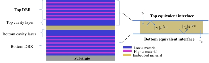
Figure 1 schematically shows the 2D materials embedded in the DBR cavity. The cavity consists of the top and bottom DBRs and a cavity layer. The basic structure can be written as (LH)mxL E yL (HL)m,L and H representing the low and high refractive index materials with thicknesses of λ0/(4×nL) and λ0/(4×nH),respectively. λ0 is the designed wavelength. E stands for embedded 2D materials. m is the number of DBR pairs. x and y control the thickness of the spacer layer. In this paper,SiO is the low n material of L and Si is the high n material of H. Black phosphorus is chosen as 2D material,which has good luminescence properties in the mid-infrared wavelength. The designed wavelength is 3.6 μm. In this calculation,the refractive indices of Si and SiO are extracted with the ellipsometry method and the absorption and dispersion of embedded materials are not considered. [17]
Figure 1.The schematic diagram of the DBR cavity and its equivalent interface
Any optical multilayer can be replaced by a virtually equivalent interface,as shown on the right of Fig. 1. The top DBR and top cavity layer are equivalent to the top equivalent interface. The bottom DBR and bottom cavity layer are equivalent to the bottom equivalent interface. Without considering the influence of substrate,the media on both sides of the film are assumed to have the same admittance,so we obtain the transmittance as:
,Let, , ,So, , ,
,,, are the transmission coefficients and reflection coefficients of the equivalent interfaces,respectively. , are the reflection phases of the equivalent interfaces and is the propagation phase.
Let’s simplify it further,
, ,, , .
The position of the maximum transmittance,also the central wavelength,is determined by the following equation:
, ,
and are the reflection phases of the top and bottom equivalent interfaces. So according to Eq. (8),when the embedded material remains unchanged,the resonant wavelength is related to the reflection phase of the top and bottom equivalent interfaces.
For the reflection phase of the top interface,it can be calculated according to TMM as follows.[18,19]
Supposing that the top DBR and the top cavity layer compose a j-th layer film,the admittance of the lower surface of the top equivalent interface can be written as follows according to the boundary conditions of plane electromagnetic wave propagation at the interface,
,
and are the amplitudes of the electric and magnetic fields of the incident wave,respectively. is the phase thickness of the film layer. is the admittance of the -th layer film and K is the number of films. There are only forward waves and no backward waves,corresponding to /=. So,
.
Let B= and C= represent the normalized electric and magnetic fields of the equivalent interface,then one can get:
.
For - polarized waves and- polarized waves,the phase thickness of the film layer is
,
the angle of refraction is determined by the refraction theorem. and are the refractive index and physical thickness of the -th layer film,respectively. is the admittance of the incident medium,which is considered a positive real number. Then there is
,
and of Eq. (8) can be expressed by Eq. (13). Therefore,when we change the embedded position,the thickness of the first layer of the equivalent interface is changed,which in turn changes the reflection phase according to Eq. (13). And then according to Eq. (8),the reflection phases of the top and bottom equivalent interfaces change as the resonant wavelength changes.
2 Results and discussion
2.1 The effect of embedded position on the resonant mode
The transmission spectra of embedded material at different positions are studied first. In this part,the only variable is the position of the embedded material. Other parameters such as the number of DBR pairs,embedded material thickness and cavity layer thickness are fixed. The specific structure is (LH)6xL E (8-x)L (HL)6. The total thickness of the cavity layer is 8L and the thickness of E is 50 nm. Figure 2 (a) shows the transmissivity spectra when they are located in different positions. The resonant mode keeps the same when the position of embedded material is in the even (or odd) cavity layer (x is an even or odd number) as shown in Fig. 2(a). This is because the 2L is the period of the changed cavity layer. The reflection phase difference of the equivalent interface is 2π,so the resonant mode does not change either. However,the resonant mode changes periodically with positions. The resonant wavelength is minimum when embedded in the position of an even cavity layer,and redshifts to the maximum when embedded in the position of an odd cavity layer. Therefore,there is a maximum peak shift (MPS) when embedded in a 2D material and the resonant wavelength is the smallest when embedded in an even cavity layer,and redshift occurs when embedded in other positions. This is caused by the reflection phase variation and the phase difference between the even and the odd layer is π. Figure 2 (b) shows the change rule of the resonant mode from the odd layer to the even layer. We can find that the redshift of the resonant mode displays gradually as the embedded position increases. When the embedded position is in an odd number layers,the MPS occurs. Although the total physical thickness of the cavity layer is constant,the resonant peak periodically shifts as the same material is embedded in different positions. This represents that the strongest coupling position has changed because of the different embedded positions. Therefore,the electric field distribution along the direction of incidence is calculated at different positions as shown in Fig. (3).
Figure 2.(a) The transmission spectra of embedded materials with the same thickness (50 nm) at different locations,(b) the variations of resonant modes with the same thickness (50 nm) at different embedded locations
Figure 3(a) shows the distribution of the electric field in the F-P cavity without the embedded material at the designed wavelength,which is a typical standing wave mode. There are four positions with the strongest electric field intensity in the cavity layer with a cavity of 8L. If the embedded material is very thin,much less than the cavity layer thickness,the choice of the embedded location is very important. Figures 3(b) and 3(c) are the distributions of the electric fields in the cavity when the same thickness of material is embedded in an even and an odd layer at the resonant wavelength,respectively. In Fig. 3(b),we can see that the embedded material is placed in an even layer with the minimum electric field,which is the worst position for the light-matter interaction. On the contrary,when the gain material is embedded in an odd layer,the coupled electric field is the strongest at the resonant wavelength of 3.65 μm,which is the best position for the light-matter interaction. Figure 3(d) is the distribution of electric field in the DBR cavity when the material embedded in an odd layer at the designed wavelength of 3.6 μm,whose intensity is low. This result shows that the cavity has a good ability to localize light at the resonant wavelength. According to the above four kinds of electric field distribution,as shown in Fig. 3,we can see that the basic mode in the cavity does not change,but the resonant mode varies when the material is embedded in different positions. Therefore,we can speculate the embedded position of the material and calculate the coupling efficiency based on the electric field at a location after testing the transmission spectrum. It is necessary to study the interaction between light and matter. At the same time,we can design the embedded position to tune the resonant wavelength. This is a simple and efficient way to fabricate integrated optical devices. Therefore,we can choose to embed 2D materials in the position with the strongest coupling to enhance the interaction between light and matter or embed materials in the weakest position to reduce the absorption loss and lower the threshold power of devices in practical applications.
Figure 3.(a) The electric field distribution without embedding (λ = 3.6 μm),(b) the electric field distribution embedded in 4L (λ = 3.64 μm),(c) the electric field distribution embedded in 3L (λ = 3.65 μm),(d) the electric field distribution embedded in 3L (λ = 3.6 μm)
2.2 The effect of the number of DBR pairs on the resonant mode
The number of DBR pairs is a key parameter for DBR performance,therefore we discuss the changes of the resonant mode under different DBR pairs as shown in Fig. 4. In this part,the variable is mainly the number of DBR pairs which is considered under two extreme positions. Other parameters such as the embedded material thickness and the cavity layer thickness are fixed. The specific structure is (LH)mxL E (8-x) L (HL)m. The total thickness of the cavity layer is 8L and the thickness of E is 50 nm. The resonant modes of odd and even layers do not change as shown in Fig. 4. When the DBR pairs vary from 4 to 8 pairs,which means the number of DBR pairs has little to do with changing the resonant mode. For each LH stack that is propagated by light,the reflection phase changes by 2π. So,the resonant wavelength will not change according to Eq. (8). However,the transmissivity decreases gradually with the increase of the DBR pair number. The full width at half maximum (FWHM) of resonant peak also decreases with the increase of the DBR pair number,while the quality factor increases correspondingly. Although these two parameters have no effect on the resonant mode,they still mutually restrict the quality of the cavity,which should be considered in the process of light-matter interaction.
Figure 4.Transmission spectra of the cavity under different numbers of DBRs with the cavity layer thickness 8L and the embedded material thickness 50 nm
2.3 The effect of the cavity layer thickness on the resonant mode
The cavity layer thickness is important to the localization of the electric field and the resonant mode can be changed by tuning the cavity layer thickness. In this part,the influence of the cavity layer thickness on the resonant mode under two extreme positions is investigated. Other parameters such as the embedded material thickness and the number of DBR pairs are fixed. The specific structure is (LH)6xL E y L (HL)6. The number of DBR pairs is set as 6 and the thickness of E is 50 nm. The cavity layer thickness is changed from 2 to 8 (x + y =2,4,6,8). The MPS is calculated as shown in Fig. 5(a). We can see that the MPS becomes smaller with the increase of the cavity layer thickness as shown in Fig. 5(b). The propagated phase is smaller when the cavity layer thickness is thinner according to Eq. (12). The maximum shifts and the cavity layer thickness are fitted using an inversely proportional relationship,which is consistent with Eq. (8). Therefore,the resonant peak can be selected by adjusting the cavity layer thickness. Given the effect of the embedded position on the resonant mode,the strongest coupling of the selected resonant mode can be achieved by tuning these two factors.
Figure 5.(a) The cavity transmissivity with different cavity thicknesses,(b) the maximum peak shifts vary with different cavity thicknesses
2.4 The effect of the embedded material thickness on the resonant mode
The influence of the embedded material thickness is also important on the resonant mode. Therefore,it is studied theoretically since single or low layer material is very difficult to be controlled freely in experiments. The variable here is mainly the embedded material thickness under two extreme embedded positions. Other parameters such as the cavity layer thickness and the number of DBR pairs are fixed. The specific structure is (LH)6xL E (8-x) L (HL)6. We find that there is a linear relationship between the MPS of cavity mode and the thickness of embedded material in a limited thickness range,as shown in Fig. 6. The resonant mode mainly changes with the embedded material thickness by tuning the propagation phase,similar to the cavity layer thickness. Therefore,such a property can be used to select the modes that can be coupled precisely for coupling by changing the embedded material thickness.
Figure 6.The MPS of the cavity mode varies with the thickness of the embedded material
In summary,the effects of the embedded materials on the cavity resonant mode in DBR cavities have been studied intensively. The embedded position,number of DBRs pairs,cavity layer thickness and embedded material thickness are four key parameters that affect the resonant mode selection and coupled electric field distribution. The cavity resonant mode changes periodically with the embedded positions with a change period of 2L. Therefore,there is an MPS with a period that decreases with the increase of the cavity layer thickness. It is also proportional to the embedded material thickness when it is thin. One can control the material embedded in different positions of the cavity or the cavity layer thickness to tune the resonant wavelength and achieve the strongest light-matter interaction. Although the number of DBR pairs does not affect the resonant mode,it still plays an important role in the localization of the light field. These results provide guidance for precise optical devices and analysis of experimental phenomena,which can be applied to different wavelength ranges of DBR cavity structures.