1National Laboratory of Solid State Microstructures, School of Physics, and College of Engineering and Applied Sciences, Nanjing University, Nanjing 210093, China
2State Key Laboratory of Modern Optical Instrumentation, Department of Optical Engineering, Zhejiang University, Hangzhou 310027, China
3Department of Physics, University of Arkansas, Fayetteville, Arkansas 72701, USA
Xiaoyang Huang, Shuwei Dai, Pengfei Xu, Yongmei Wang, Qing Yang, Yong Zhang, Min Xiao, "Resonant and nonresonant second-harmonic generation in a single cadmium sulfide nanowire," Chin. Opt. Lett. 15, 061901 (2017)
Copy Citation Text
We experimentally investigate the resonant and nonresonant second-harmonic generation in a single cadmium sulfide (CdS) nanowire. The second-order susceptibility tensor is determined by analyzing the forward second-harmonic signals of the CdS nanowire. Our results show that (1) at a nonresonant input wavelength of 1050 nm; (2) at a resonant wavelength of 740 nm. The difference can be attributed to the polarization-dependent resonance.
Cadmium sulfide (CdS) nanocrystals have been attracting considerable attention due to its excellent optical and electronic properties. It is a member of wide direct band gap () semiconducting compounds and possesses large optical nonlinearities, which make it extensively useful in linear and nonlinear optoelectronic devices. In the past several years, many researchers have synthesized different CdS nanostructures, such as nanoparticles, nanoribbons, and nanowires through various growth methods[1–8]. The optical properties of such CdS nanostructures, including photoluminescence, absorption, and lasing, have been well studied[4–12]. Benefiting from their large second-order nonlinear response, CdS nanowires have been proven to be very useful in efficiently realizing nonlinear optical effects, such as optical correlation[13] and nonlinear optical mixing[14]. Also, the optical limiting properties of CdS nanowires were reported recently[15]. However, the second-order nonlinear susceptibilities of a single CdS nanowire have not been well investigated.
Second-harmonic (SH) generation arises from the second-order nonlinear polarization in a nonlinear optical crystal[16–19]. By investigating the dependence of the SH intensities on the excitation polarizations, the second-order nonlinear susceptibility of a single CdS nanowire can be determined[20–25]. The generated SH waves from such nanowires can be analyzed by using near-field scanning optical microscopy[26] or far-field microscopic imaging[27]. Both methods are based on the detection of the back-reflected SH signal. Compared to the forward SH emission, the back-irradiated SH emission has a much shorter coherence length and a much lower intensity, which will reduce the quality of the SH signals and the measurement accuracy. In this work, we utilize a forward SH scattering method[28,29], which is ideal for characterizing nanostructures with similar sizes to the wavelengths involved, to characterize the second-order susceptibility tensors of single CdS nanowires. In addition, it has been reported that the second-order nonlinear optical response of a nanowire can be significantly influenced by the resonant excitation (i.e., the SH photon energy is above the bandgap of the semiconductor nanowire)[30,31]. In the experiment, we have investigated the SH generation of a single CdS nanowire in the resonant and nonresonant wavelengths for comparison. Our experimental results provide useful and essential information for further design of nanophotonic devices based on CdS nanowires.
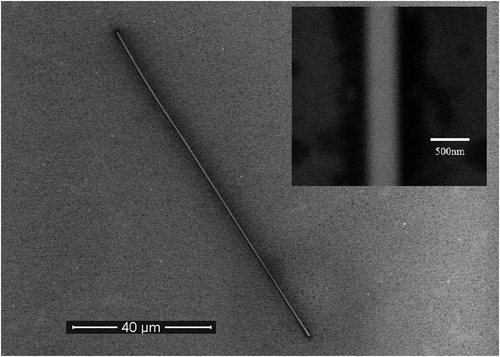
The CdS nanowires are synthesized by the chemical vapor deposition (CVD) method. An alumina boat with 2 g CdS powder (Alfa Aesar, 99.99% purity) is placed at the center of the quartz tube, which is mounted inside a single-zone furnace. Silicon wafers coated with about a 2-nm-thick gold film are placed downstream of the alumina boat to sever as the substrates of the deposited CdS nanowires. During the growth period, high purity nitrogen gas is introduced into the quartz tube at a flow rate of 175 SCCM to purge oxygen from the tube and maintain the pressure at 720 mbar. Meanwhile, the temperature of the heat area in the furnace is set at 830°C for 1 h. After growth, the furnace naturally cools down to room temperature. Then, the nanowires are transferred to a fused silica substrate. A typical nanowire, as shown in Fig. 1, has a diameter of about 500 nm and a length of about 100 μm. The experimental setup is shown in Fig. 2. A mode-locked Ti:Sapphire laser served as the fundamental field. The repetition rate is 80 MHz, and the temporal width is 75 fs. The incident beam is focused by a lens () onto the center of the single CdS nanowire. The diameter of the focusing spot is close to the length of the nanowire. A short-pass filter is placed after the sample to eliminate the fundamental wave. The transmitted SH signal is collected by another lens and is detected by a spectrometer. We use a chopper and a lock-in amplifier to further enhance the signal-to-noise ratio. A half-wave plate is used to control the polarization of the incident fundamental beam, which is placed on a rotating mount driven by an electric motor. A Glan–Taylor prism is used to analyze the polarization of the SH signal. Under this experimental configuration, it is convenient to measure the SH intensities as changing the polarization of the fundamental wave.
Sign up for Chinese Optics Letters TOC. Get the latest issue of Chinese Optics Letters delivered right to you!Sign up now
Figure 1.SEM image of the single CdS nanowire sample. As shown in the inset, the diameter of the nanowire is about 500 nm.
Figure 2.Experimental setup. M, mirror; CH, chopper; HWP, half-wave plate; L1 and L2, lens; LF, long-pass filter; S, sample; SF, short-pass filter; P, polarizer; PMT, photomultiplier tube. and indicate the - and -polarizations, respectively. , , and are the crystallographic axes of the CdS nanowire.
By applying the vacuum-substrate-nanowire-vacuum four layers model[28], the transmitted SH fields can be written as where and represent the wave vector components of the SH wave and the fundamental wave in the nanowire along the normal direction, respectively. is the Fresnel factor of the - or -polarized SH wave from the nanowire to the vacuum, is the diameter of the nanowire, and are the unit vectors along the and directions. As illustrated in Fig. 2, the direction is parallel to the axis of the CdS crystal, while the direction is parallel to the axis under normal incidence. The second-order nonlinear susceptibility tensor of wurtzite CdS (6 mm point group) can be represented as which has five nonzero elements, i.e., , , and . Then, the SH fields in Eqs. (1a) and (1b) can be rewritten as with , , , and . Here, are scaling factors, are Fresnel transmission coefficients for the fundamental wave from the air to the nanowire, and are refractive indices of CdS at the SH and fundamental frequencies, is the incidence angle, and represents the polarization of the incident beam. The dependence of the transmitted SH intensities on the polarization of incident beam can be written as where the parameters , , and can be fitted by the experimental results. The ratios of and satisfy the equation
First, we investigate the SH generation of the CdS nanowire in a nonresonant wavelength of 1050 nm. In order to determine in Eq. (4), we carry out the experimental measurements under normal incidence. The experimental results are shown in Fig. 3(a), which can be well fitted by using Eqs. (3a) and (3b). By substituting the obtained fitting parameters and into Eq. (4), it is easy to solve out the ratio of . The absolute values of the susceptibilities are determined by comparing the SH intensity from the CdS nanowire with that from a Z-cut quartz reference plate. The [1000] direction of the quartz is oriented parallel to the incidence plane. Under normal incidence of a -polarized fundamental wave (i.e., , ), we have where and are corresponding Fresnel transmission coefficients of the fundamental waves propagating from air to quartz and CdS nanowire, respectively. and are the scaling factors for quartz and CdS nanowire, respectively. By comparing Eqs. (5a) and (5b), it is easy to obtain
Figure 3.Experimentally measured -polarized and -polarized SH intensities as a function of the polarization of the normal incident fundamental wave at (a) 1050 and (b) 740 nm. The theoretical fits using Eq. (3a) and (3b) are in good agreement with the experimental results.
In our experiment, the ratio of of the single CdS nanowire at 1050 nm is determined to be . The absolute value of is 15.5 pm/V. The sign of is negative, which is similar to that of single wurtzite ZnO nanowires[28,32]. The second-order susceptibilities of bulk CdS crystal measured by Miller et al. are , and at a fundamental wavelength of 1058 nm[33,34]. The reported values of CdS films are , and at 1064 nm[34]. Both studies did not consider the signs of the coefficients. In comparison to the CdS nanowire used in our experiment, the absolute values of the nonlinear coefficients are of the same order of magnitude. The value of in a CdS nanowire is a little smaller than that of the CdS film or bulk crystal, which may result from the imperfect crystal quality of the nanowire. The ratio of in the nanowire is quite different from the value of the CdS film or bulk crystal, which can be attributed to the crystal lattice distortion in the nanowire. The asymmetry at the surface of the nanowire also contributes to the SH signals[23], and therefore, causes certain changes in the ratio of .
To investigate the impact of the resonance on the second-order susceptibilities of the CdS nanowire, we conduct the experiment at a fundamental wavelength of 740 nm. Figure 4 shows the measured emission spectrum after filtering out the fundamental wave. One peak at 370 nm is the SH wavelength. The other peak locates at about 510 nm, which results from the two-photon fluorescence (TPF) process. Clearly, the spectrum in Fig. 4 indicates a resonant experimental condition. Under such resonant excitation, the competition of the TPF process usually results in a significant change in the second-order nonlinear susceptibility of the semiconductor nanowire[30,31]. The measurement of the second-order susceptibilities of the CdS nanowire is performed by detecting the SH signal at 370 nm. The experimental arrangement is the same as described above. The measured dependences of the - and -polarized SH intensities on the fundamental polarization under normal incidence are shown in Fig. 3(b). The theoretical fitting by using Eq. (4) gives at 740 nm. Clearly, it is quite different from the nonresonant value of at 1050 nm. This can be explained by the fact that the resonance strength is dependent on the input polarization. As shown in Fig. 4, the TPF peak at 510 nm under a -polarized excitation is much stronger than that with an -polarized fundamental beam. To precisely determine the absolute values of the nonlinear susceptibilities of the CdS nanowire at 740 nm, one must consider the two-photon absorption of the fundamental wave and the linear absorption of the SH wave (which are neglected in the nonresonant case) in the theoretical model.
Figure 4.Emission spectra from a single CdS nanowire excited by a -polarized (solid line) and -polarized (dashed line) femtosecond laser (740 nm).
In conclusion, we experimentally study the second-order susceptibility tensor of a single CdS nanowire synthesized by the CVD method. The experimental measurements are performed by recording the dependence of the transmitted SH signal on the polarization of the fundamental wave. At a nonresonant input wavelength of 1050 nm, we obtain . The corresponding absolute value of is measured to be 15.5 pm/V. At a resonant wavelength of 740 nm, the value of becomes , which results from the polarization-dependent resonance. Our results provide useful information for future designs of nonlinear optical devices based on CdS nanowires.