• Chinese Optics Letters
  • Vol. 20, Issue 2, 023602 (2022)
Chuangye Zhang, Changjun Min*, Yuquan Zhang, Yanan Fu, Ling Li, Yulong Wang, and Xiaocong Yuan**
Author Affiliations
  • Nanophotonics Research Center, Shenzhen Key Laboratory of Micro-Scale Optical Information Technology & Institute of Microscale Optoelectronics, Shenzhen University, Shenzhen 518060, China
  • show less
    DOI: 10.3788/COL202220.023602 Cite this Article Set citation alerts
    Chuangye Zhang, Changjun Min, Yuquan Zhang, Yanan Fu, Ling Li, Yulong Wang, Xiaocong Yuan. Detection of cylindrical vector beams with chiral plasmonic lens[J]. Chinese Optics Letters, 2022, 20(2): 023602 Copy Citation Text show less

    Abstract

    The cylindrical vector beam (CVB) has been extensively studied in recent years, but detection of CVBs with on-chip photonic devices is a challenge. Here, we propose and theoretically study a chiral plasmonic lens structure for CVB detection. The structure illuminated by a CVB can generate single plasmonic focus, whose focal position depends on the incident angle and the polarization order of CVB. Thus, the incident CVB can be detected according to the focal position and incident angle and with a coupling waveguide to avoid the imaging of the whole plasmonic field. It shows great potential in applications including CVB-multiplexing integrated communication systems.

    1. Introduction

    As an important part of modern optics, singular optics has attracted more and more research attention in recent years[13]. Optical phase singularity and polarization singularity originate from the uncertainty of phase and polarization in the light field, and their corresponding representative beams are the well-known optical vortex (OV) and cylindrical vector beam (CVB), respectively. CVB is a kind of singular optical beam with spatially non-uniform but rotational-symmetric polarization state, therefore forming a polarization singularity in the center of the beam’s cross section with a donut-shaped intensity pattern[4,5]. Due to the novel properties in polarization, CVB has been widely applied in many optical research fields, such as optical tweezers[6,7], surface plasmon polariton (SPP) excitation and modulation[8], fiber laser of the CVB[911], tip enhanced Raman spectroscopy[12,13], and others. Besides the well-known radial and azimuth polarized beams[14], CVB includes a high-order vectorial polarization state[15]. Since CVBs of different polarization orders are orthogonal to each other, the polarization order of CVBs has already been employed as a new degree of freedom in CVB-multiplexing optical communication systems[16,17].

    In order to develop more applications of CVB, detection of the CVB’s polarization order becomes an important research hotspot not only in free-space applications, but also in fiber and integrated optical systems. Traditional CVB detection methods usually include parallel-aligned liquid crystal display[18], triangle common path interferometry[19], and thermally tuned q-plates[20]. However, these traditional methods have disadvantages, such as the requirements of multiple optical elements and large system volume, and therefore are not suitable for applications in integrated optical systems. For example, the integrated CVB-multiplexing optical communication systems require CVB detection devices with micro/nano-scale size to minimize the volume of the system. Thus, it is still a challenging work to detect CVBs with micro/nano-scale optical devices.

    In this Letter, we propose and theoretically study a new method for CVB detection by using an on-chip microscale structure of a chiral plasmonic lens. In such a structure, single SPP focus can be excited by an incident CVB with certain polarization order, and its focal position is determined by both the incident angle and the polarization order of the CVB. Based on analyzing the relationship among the three key factors (focal position, incident angle, and polarization order), the polarization order of incident CVBs can be detected by measuring the other two. Furthermore, to avoid imaging the complete SPP field to get the focal position, we design a dielectric waveguide close to the chiral plasmonic lens to couple the energy of SPP focus, and thus the detection of CVBs can be simply realized by monitoring the optical signal transmitted through the waveguide. Our numerical results agree well with the analytical model and demonstrate that detection of CVB can be achieved by the proposed structure. This method could be of great significance to the development of miniaturization and integration of singular optical devices.

    2. Principle of the Chiral Plasmonic Lens

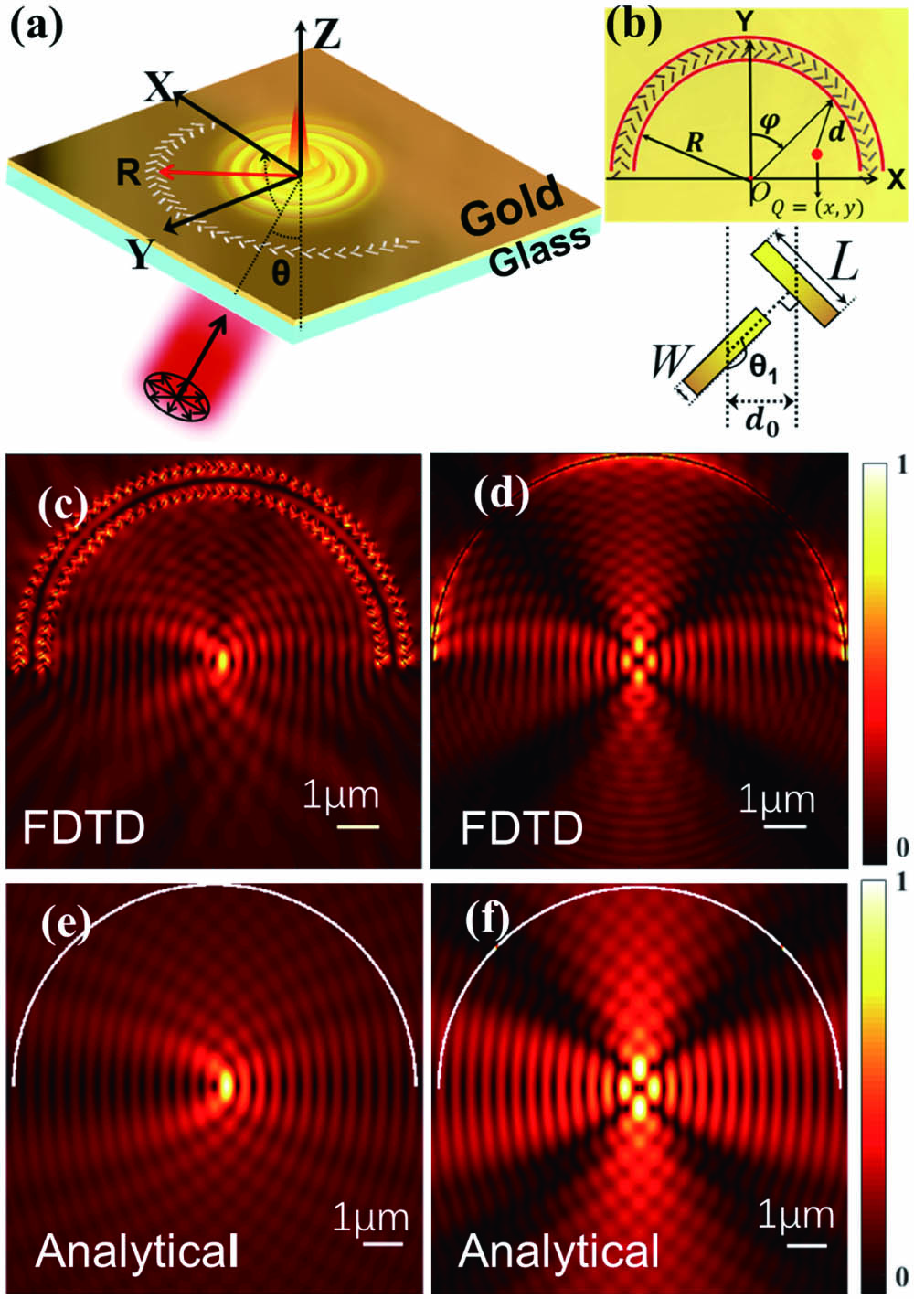
    Figure 1(a) shows the schematic diagram of the proposed structure of the chiral plasmonic lens, which is a semicircular shape composed of multiple spin-sensitive unit cells of nano-slits on a 200-nm-thick gold film and a glass substrate. A 633 nm wavelength plane-wave CVB is incident from the bottom in the xz plane with an incident angle θ to the z axis. Due to the scattering of the nano-slits in the semicircular-shaped structure, SPP waves are excited and propagate on the gold surface with a converging wavefront and then generate a focal field of SPP on the gold film. The details of structure parameters and single unit cell are shown in Fig. 1(b). Each unit cell includes two mutually perpendicular nano-slits with θ1=135° and has been proved to show chiral response to the spin polarization state (left/right circular polarization) of incident light[21]. The slit length is L=240nm, and the width is W=60nm. The distance d0 between the two slits is 600 nm, and the radius of the semicircular structure is R=4μm.

    (a) Schematic diagram of the chiral plasmonic lens. (b) Structural parameters (up) and single unit cell with two slits (down). (c) FDTD simulated result of SPP field in the xy plane excited by the chiral plasmonic lens. Two layers of the structure are used to enhance the SPP field. (d) FDTD simulated result of the SPP field excited by a single semicircular slit with 100 nm width and radius R = 4 µm. (e), (f) The analytical model results corresponding to (c), (d). In (c)–(f), the order of CVB is m = 3, and the incident angle θ = 0°.

    Figure 1.(a) Schematic diagram of the chiral plasmonic lens. (b) Structural parameters (up) and single unit cell with two slits (down). (c) FDTD simulated result of SPP field in the xy plane excited by the chiral plasmonic lens. Two layers of the structure are used to enhance the SPP field. (d) FDTD simulated result of the SPP field excited by a single semicircular slit with 100 nm width and radius R = 4 µm. (e), (f) The analytical model results corresponding to (c), (d). In (c)–(f), the order of CVB is m = 3, and the incident angle θ = 0°.

    To demonstrate the function of the designed structure, we consider a CVB with polarization order m=3 [Jones vector shown in Eq. (1) and polarization state shown in Fig. 2(c)] normally illuminating onto the structure from the bottom, and then we compare the generated SPP focal fields in two cases, including a traditional plasmonic lens [single semicircular slit shown in Fig. 1(d)][22] and the proposed chiral plasmonic lens [Fig. 1(c)], obtained by the 3D finite-difference time-domain (FDTD, Lumerical FDTD Solutions) simulation method. In Fig. 1(c), we use double layers of the chiral plasmonic lens with a distance of SPP wavelength λSPP=600nm to enhance the focal intensity. Through the comparison between Figs. 1(c) and 1(d), it can be observed that, due to the non-uniform polarization distribution of CVB, multiple SPP foci are generated in the center by the traditional plasmonic lens, but a stronger single SPP focus is formed by the chiral plasmonic lens.

    (a)–(c) Polarization distribution (black arrows) of CVB with m = −2, 1, and 3, and the corresponding (d)–(f) SPP field is excited by the above three CVBs. The white line indicates the center position (x = 0). (g) The SPP focal field profile in the x axis with different order m. (h) The relationship between SPP focal position in the x axis and the CVB order m.

    Figure 2.(a)–(c) Polarization distribution (black arrows) of CVB with m = −2, 1, and 3, and the corresponding (d)–(f) SPP field is excited by the above three CVBs. The white line indicates the center position (x = 0). (g) The SPP focal field profile in the x axis with different order m. (h) The relationship between SPP focal position in the x axis and the CVB order m.

    Next, we theoretically explain why the chiral plasmonic lens can generate single SPP focus rather than multiple foci. In fact, an m-order CVB can be divided into two different OV beams, including a right-handed circularly polarized OV beam with topological charge of m and a left-handed circularly polarized OV beam with topological charge of m. The corresponding Jones vector of the CVB is shown in Eq. (1), where m is the polarization order of the CVB, φ is the azimuthal angle, and α is the initial phase:ECVB=(cos(mφ+α)sin(mφ+α))=12exp[i(mφ+α)](1i)+12exp[i(mφ+α)](1i).

    Owing to the chiral response of the nano-slits to the spin polarization state of incident light[21], the two orthogonal spin-polarized OV beams in Eq. (1) lead to different performances in SPP propagation. Specifically, in the chiral plasmonic lens, the left-handed OV part of the CVB will excite SPPs propagating towards the center of the semicircle and forming the single focus, while the right-handed OV part will excite SPPs propagating outward and diverging. Thus, whatever the order of the CVB is, a single SPP focus can always be generated by the left-handed OV part, and its focal position can be modulated by the topological charge m (also the order of CVB)[22].

    To further verify the different performances in Figs. 1(c) and 1(d), we calculate the SPP focal fields of the two cases with the analytical method. Considering that an incident OV beam has an electric field of Eexp(ijφ)exp(r2) (r is the distance of each point in the beam cross section to the center), the focal field of SPPs excited by the OV beam with a plasmonic lens can be expressed as[23]E(x,y)cexp(ikSPP)Rππ/2π/2exp(ijφ)U(φ)exp(ikSPP)ddφ,where j=σ+l is the total angular momentum, σ is the spin angular momentum of the OV beam (σ=1 for left circular polarization, σ=1 for right circular polarization), and l is the topological charge of the OV. kSPP is the wave vector of the excited SPP, U(φ) is the complex amplitude on the plasmonic lens, and d is the distance from the reference point Q(x,y) to each point on the plasmonic lens, as shown in Fig. 1(b). For the chiral plasmonic lens, only the left-handed OV part of the CVB generates the focal SPP field, so we have σ=1, l=m, and the total angular momentum j=m1. In the case of CVB with order m=3 (j=2), the SPP focal field calculated by Eq. (2) is shown in Fig. 1(e), which is almost the same as the FDTD result in Fig. 1(c). In contrast, for the traditional plasmonic lens, both the left-handed and right-handed OV parts can generate an SPP focal field; hence, the two SPP focal fields will interfere to form the multiple SPP foci. The SPP focal field for the traditional plasmonic lens calculated by Eq. (2) is shown in Fig. 1(f), agreeing well with the FDTD result in Fig. 1(d). Both FDTD and analytical results in Figs. 1(c)1(f) prove that the proposed chiral plasmonic lens can generate single SPP focus, which can be used in the CVB detection studied in the following section.

    3. Results of CVB Detection

    Several previous works have demonstrated that the SPP focal field can be used to discriminate OV beams[24,25]. Here, we find it also can be used to detect the order of CVB. To prove it, we use the FDTD simulation method to study the effect of the CVB order on the SPP focal position, as shown in Fig. 2. In Figs. 2(a)2(c), we compare three different cases of CVB (m=2, 1, and 3, α=0) normally illuminating on the structure (θ=0°). When the order m changes, the polarization distribution in the beam cross section changes, and the corresponding topological charges of the two divided OV beams also change according to Eq. (1). Since the topological charge of the left-handed OV part of the CVB determines the initial phase of excited SPPs, the wavefront of propagating SPPs is different at different orders m, resulting in different focal positions of SPPs. Figures 2(d)2(f) show the FDTD simulated SPP focal fields in the three cases of CVB. For the case of m=1, the CVB is the standard radially polarized light, and its left-handed OV part (σ=1, l=1) has the total angular momentum j=σ+l=0, and thus the SPP focus is located at the center position (x=0). For the other two cases of the CVB with order m=2 and 3, the left-handed OV part has the total angular momentum j=3 and 2 in generation of the SPP focal field, respectively, leading to a shift of SPP focus in the x direction[21]. To further quantify the shift of SPP focus as the order m changes, in Fig. 2(g), we show the intensity profiles of SPP focus along the x axis (y=0) with different values of order m=2to3. The SPP focus is evenly distributed in the x axis and moves to the right with the increase of m. In Fig. 2(h), we present a linear relationship between the position of SPP focus and the CVB order m, and the shift distance of SPP focus is about 120 nm between two adjacent orders.

    Besides the polarization order m, the SPP focal position is also affected by the incident angle θ. Because an additional tilted phase factor can be induced by the incident angle θ to the incident light, the excited SPP could have a tilted wavefront, also leading to a shift of SPP focus in the x direction. To study the effect of incident angle θ on the SPP focal position, we fix the CVB order m=2 and change the incident angle to calculate the SPP focal field, as shown in Figs. 3(a)3(c). For the case of θ=1.1° [Fig. 3(b)], we can observe that the SPP is focused at the center point (x=0). For the other two cases of θ=2° (3°) [Figs. 3(a) and 3(c)], the SPP focus moves to the right (left) side in the x axis due to the tilted phase factor of incident light. In Figs. 3(d) and 3(e), we show the intensity profiles of the SPP focus along the x axis, proving that the SPP focus moves to the left with the increase of angle θ. From Fig. 3(e), we find that 1° change of θ leads to a shift distance about 120 nm of SPP focus. Like the order m, here the incident angle θ also shows a linear relationship with the position of SPP focus.

    (a)–(c) SPP field excited by the CVB with different incident angle θ. The white line indicates the center position (x = 0). (d) The SPP focal field profile in the x axis with different incident angle θ. (e) The relationship between SPP focal position in the x axis and the incident angle θ.

    Figure 3.(a)–(c) SPP field excited by the CVB with different incident angle θ. The white line indicates the center position (x = 0). (d) The SPP focal field profile in the x axis with different incident angle θ. (e) The relationship between SPP focal position in the x axis and the incident angle θ.

    Through the above results in Figs. 2 and 3, we find that the incident angle θ and CVB order m have similar shift effect on the SPP focal position. Moreover, for a fixed CVB order m, there must be a corresponding value of θ that can offset the shift effect of m and thus pull the SPP focus back to the center (x=0). For example, in Fig. 3(b), the shift effect of the CVB order m=2 is counteracted by the incident angle θ=1.1°; hence, finally, the SPP focus appears at the center position.

    Based on the offset relationship between the incident angle θ and the CVB order m in the shift of SPP focal position, we propose a method to detect the order m by changing the incident angle θ to find the perfect offset angle that can pull the SPP focus back to the center. Although, according to the results in Fig. 2, the CVB order m can be directly detected by imaging the whole SPP focal field with a super-resolved microscopy system [e.g.,  near-field scanning optical microscope (NSOM) in a previous report[26]]; it has low-speed/efficiency, and it is quite difficult to scan the whole SPP field to find the accurate focal position. In order to avoid imaging of the whole SPP field with a complicated microscopy system, here we propose an on-chip method by placing a silica waveguide (width of 200 nm and height of 300 nm) near the center point of the chiral plasmonic lens to couple the energy of SPP focus into the waveguide, as schematically shown in Fig. 4(a). A similar waveguide coupling method has been proved for multiplexing of OV beams[27]. For a fixed CVB order m, when we gradually change the incident angle θ to the perfect offset angle, the SPP focus will be pulled back to the center and provide the maximum coupling efficiency to the waveguide. Thus, we only need to monitor the transmission through the waveguide as the angle θ changes, and, once the transmission reaches the peak value, the CVB order m can be determined by the corresponding incident angle θ at the transmission peak. For example, in Figs. 4(b) and 4(c), we show the Poynting vector (Py) distribution in the SPP focal field and in the waveguide at different incident angle θ. When the SPP focus is pulled back to the center, the coupling efficiency between the SPP focus and the waveguide gets the maximum value, so the energy transmission inside the waveguide also reaches the maximum [Fig. 4(b)]. Otherwise, the energy coupled into the waveguide is much weaker, as shown in Fig. 4(c).

    (a) Schematic diagram of waveguide focus coupling. (b), (c) Influence of SPP focus position on waveguide coupling (the white line is the waveguide area, and the result in the figure is Py). (d) Normalized transmission of the waveguide at different CVB orders and different incident angles. (e) The linear relationship corresponding to the peak point in (d).

    Figure 4.(a) Schematic diagram of waveguide focus coupling. (b), (c) Influence of SPP focus position on waveguide coupling (the white line is the waveguide area, and the result in the figure is Py). (d) Normalized transmission of the waveguide at different CVB orders and different incident angles. (e) The linear relationship corresponding to the peak point in (d).

    For the detection of CVB order, in Figs. 4(d) and 4(e), we study the relationship between the CVB order m and the incident angle θ from the resultant waveguide transmission peaks. Figure 4(d) shows the waveguide transmission as a function of the incident angle θ at different order m. It proves that for different CVB order m, the transmission peak appears at different incident angle, and their relationship, as shown in Fig. 4(e), is almost a linear result. Thus, based on the results in Figs. 4(d) and 4(e), we only need to change the incident angle until the transmission through the waveguide reaches the peak, and then the order m of incident CVB can be determined according to the approximately linear relation in Fig. 4(e). This method could achieve a simpler implementation of CVB detection than scanning the whole SPP focal field with an NSOM system.

    Although this is a theoretical research work, it can be realized in experiment. In our designed structure, the chiral plasmonic lens with nano-slits can be fabricated by a focused ion beam process on gold film[21], and the dielectric waveguide can be fabricated by electron beam lithography or directly using a dielectric nanowire/nanofiber[27]. To achieve CVB detection, the structure can be placed on a high-precision angle rotator, and the CVB is incident at a fixed angle onto the structure. Through the accurate rotation of the rotary table as well as the structure, the transmission peak through the waveguide can be measured at a specific incident angle as the result in Fig. 4(d), and then the CVB order can be experimentally measured according to the angle and the result in Fig. 4(e).

    4. Conclusion

    In conclusion, we propose a microscale structure of a chiral plasmonic lens with a waveguide for detection of CVB. Owing to the spin-sensitive response of the chiral plasmonic lens, single SPP focus on gold film can be excited by incident CVB, and such an effect is verified by both the analysis model and the FDTD simulation methods. The influence of two key parameters of the incident CVB, including the polarization order m and the incident angle θ, on the SPP focus shifting and coupling to the waveguide is investigated in detail. Finally, an approximately linear relationship between the order m and angle θ at maximum transmission through the waveguide is obtained for the on-chip detection of CVB. This method has advantages of microscale device size and no requirement of imaging the SPP field with complicated super-resolved microscopy system and thus could show wide application potential in the fields of integrated optical information processing devices and on-chip optical communication systems.

    References

    [1] M. S. Soskin, M. V. Vasnetsov. Singular optics. Prog. Opt., 42, 219(2001).

    [2] M. R. Dennis, K. O’Holleran, M. J. Padgett. Chapter 5 singular optics: optical vortices and polarization singularities. Prog. Opt., 53, 293(2009).

    [3] D. Mao, Y. Zhang, C. Zeng, L. Hua, C. Wang, H. Zhang, W. Zhang, T. Mei, J. Zhao. Generation of polarization and phase singular beams in fibers and fiber lasers. Adv. Photon., 3, 014002(2021).

    [4] D. G. Hall. Vector-beam solutions of Maxwell’s wave equation. Opt. Lett., 21, 9(1996).

    [5] Q. Zhang. Cylindrical vector beams: from mathematical concepts to applications. Adv. Opt. Photon., 1, 1(2009).

    [6] Y. Zhang, C. Min, X. Dou, X. Wang, X. Yuan. Plasmonic tweezers: for nanoscale optical trapping and beyond. Light Sci. Appl., 10, 59(2021).

    [7] Y. Yang, Y. Ren, M. Chen, Y. Arita, C. R. Guzmán. Optical trapping with structured light: a review. Adv. Photon., 3, 034001(2021).

    [8] Z. Man, L. Du, C. Min, Y. Zhang, C. Zhang, S. Zhu, H. Urbach, X. Yuan. Dynamic plasmonic beam shaping by vector beams with arbitrary locally linear polarization states. Appl. Phys. Lett., 105, 011110(2014).

    [9] S. Chen, J. Li, K. I. Ueda. Cylindrical vector beam rotary Nd:YAG disk laser with birefringent crystal. Chin. Opt. Lett., 18, 121401(2020).

    [10] D. Mao, T. Feng, W. Zhang, H. Lu, Y. Jiang, P. Li, B. Jiang, Z. Sun, J. Zhao. Ultrafast all-fiber based cylindrical-vector beam laser. Appl. Phys. Lett., 9, 021107(2017).

    [11] H. Wan, J. Wang, Z. Zhang, Y. Cai, B. Sun, L. Zhang. High efficiency mode-locked, cylindrical vector beam fiber laser based on a mode selective coupler. Opt. Express, 25, 11444(2017).

    [12] H. Chen, Y. Zhang, Y. Dai, C. Min, S. Zhu, X. Yuan. Facilitated tip-enhanced Raman scattering by focused gap-plasmon hybridization. Photon. Res., 8, 103(2020).

    [13] W. Zhang, L. Zhang, C. Meng, F. Gao. Generation of nanosecond cylindrical vector beams in two-mode fiber and its applications of stimulated Raman scattering. Chin. Opt. Lett., 19, 010603(2021).

    [14] Z. Yang, Z. Wang, Y. Wang, X. Feng, M. Zhao, Z. Wan, L. Zhu, J. Liu, Y. Huang, J. Xia, M. Wegener. Generalized Hartmann–Shack array of dielectric metalens sub-arrays for polarimetric beam profiling. Nat. Commun., 107, 07056(2018).

    [15] X. Weng, L. Du, A. Yang, C. Min, X. Yuan. Generating arbitrary order cylindrical vector beams with inherent transform mechanism. IEEE Photon. J., 9, 6100208(2017).

    [16] Y. Zhao, J. Wang. High-base vector beam encoding/decoding for visible-light communications. Opt. Lett., 40, 4843(2015).

    [17] J. Fang, Z. Xie, T. Lei, C. Min, L. Du, Z. Li, X. Yuan. Spin-dependent optical geometric transformation for cylindrical vector beam multiplexing communication. ACS Photon., 5, 3478(2018).

    [18] I. Moreno, J. A. Davis, I. Ruiz, D. M. Cottrell. Decomposition of radially and azimuthally polarized beams using a circular-polarization and vortex-sensing diffraction grating. Opt. Express, 18, 7173(2009).

    [19] S. Zheng, Y. Li, Q. Lin, X. Zeng, G. Zheng, Y. Cai, Z. Chen, S. Xu, D. Fan. Experimental realization to efficiently sort vector beams by polarization topological charge via Pancharatnam–Berry phase modulation. Photon. Res., 6, 385(2018).

    [20] G. Milione, M. P. J. Lavery, H. Huang, Y. Ren, G. Xie, T. A. Nguyen, E. Karimi, L. Marrucci, D. A. Nolan, R. R. Alfano, A. E. Willner. 4 × 20 Gbit/s mode division multiplexing over free space using vector modes and a q-plate mode (de)multiplexer. Opt. Lett., 40, 1980(2010).

    [21] J. Lin, J. P. B. Mueller, Q. Wang, G. Yuan, N. Antoniou, X. Yuan, F. Capasso. Polarization-controlled tunable directional coupling of surface plasmon polaritons. Science, 340, 331(2013).

    [22] S. Mei, K. Huang, H. Liu, F. Qin, M. Q. Mehmood, Z. Xu, M. Hong, D. Zhang, J. Teng, A. Dannera, C. Qiu. On-chip discrimination of orbital angular momentum of light with plasmonic nanoslits. Nanoscale, 8, 2227(2016).

    [23] S. S. Kou, G. Yuan, Q. Wang, L. Du, E. Balaur, D. Zhang, D. Tang, B. Abbey, X. Yuan, J. Lin. On-chip photonic Fourier transform with surface plasmon polaritons. Light Sci. Appl., 5, e16034(2016).

    [24] G. Yuan, X. Yuan, J. Bu, P. Tan, Q. Wang. Manipulation of surface plasmon polaritons by phase modulation of incident light. Opt. Express, 19, 224(2011).

    [25] G. Yuan, Q. Wang, P. Tan, J. Lin, X. Yuan. A dynamic plasmonic manipulation technique assisted by phase modulation of an incident optical vortex beam. Nanotechnology, 23, 385204(2012).

    [26] K. Y. Bliokh, F. J. Rodríguez-Fortuño, F. Nori, A. V. Zayats. Spin–orbit interactions of light. Nat. Photonics, 9, 796(2015).

    [27] H. Ren, X. Wang, C. Li, C. He, Y. Wang, A. Pan, S. A. Maier. An orbital angular momentum-controlled hybrid nanowire circuit. Nano Lett., 21, 6220(2021).

    Chuangye Zhang, Changjun Min, Yuquan Zhang, Yanan Fu, Ling Li, Yulong Wang, Xiaocong Yuan. Detection of cylindrical vector beams with chiral plasmonic lens[J]. Chinese Optics Letters, 2022, 20(2): 023602
    Download Citation