• Photonics Research
  • Vol. 12, Issue 4, 784 (2024)
Yinong Xie1、2、†, Qianting Chen1、2、†, Jin Yao3, Xueying Liu1、2, Zhaogang Dong4、5, and Jinfeng Zhu1、2、*
Author Affiliations
  • 1Institute of Electromagnetics and Acoustics and Key Laboratory of Electromagnetic Wave Science and Detection Technology, Xiamen University, Xiamen 361005, China
  • 2Shenzhen Research Institute of Xiamen University, Shenzhen 518057, China
  • 3Department of Electrical Engineering, City University of Hong Kong, Hong Kong 999077, China
  • 4Institute of Materials Research and Engineering (IMRE), Agency for Science, Technology and Research (A*STAR), Singapore 138634, Singapore
  • 5Department of Materials Science and Engineering, National University of Singapore, Singapore 117575, Singapore
  • show less
    DOI: 10.1364/PRJ.514140 Cite this Article Set citation alerts
    Yinong Xie, Qianting Chen, Jin Yao, Xueying Liu, Zhaogang Dong, Jinfeng Zhu. Dielectric metasurface evolution from bulk to monolayer by strong coupling of quasi-BICs for second harmonic boosting[J]. Photonics Research, 2024, 12(4): 784 Copy Citation Text show less
    Schematic diagram for the evolution from bulk to monolayer q-BIC metasurfaces, where the symbols p, t, w, d1, d2, d3, and θ denote the period, thickness of waveguide layer, width and heights of various asymmetrical rectangular pairs, and the incident angle, respectively.
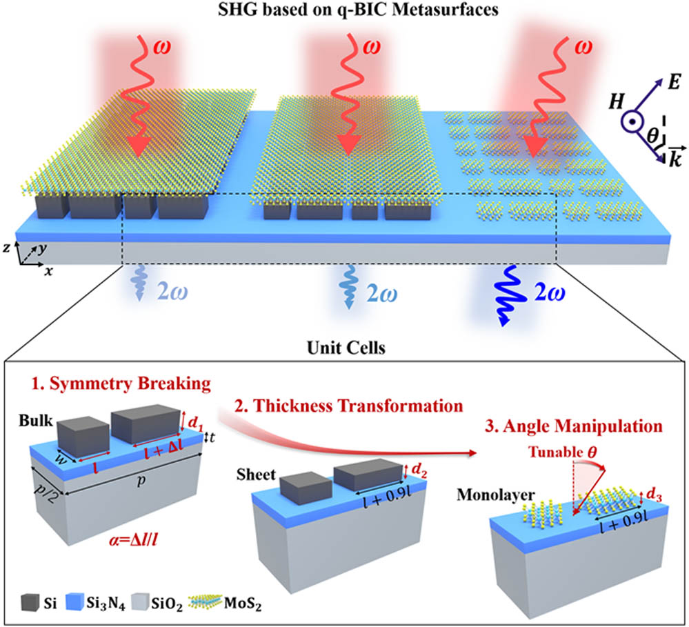
    Fig. 1. Schematic diagram for the evolution from bulk to monolayer q-BIC metasurfaces, where the symbols p, t, w, d1, d2, d3, and θ denote the period, thickness of waveguide layer, width and heights of various asymmetrical rectangular pairs, and the incident angle, respectively.
    (a) Transmittance of Si metasurface with in-plane asymmetric q-BIC as a function of α, where d1=100 nm. (b) Transmittance of Si metasurface with in-plane asymmetric q-BIC as a function of d2, where α=0.9. (c) Transmittance of metasurface as a function of MoS2 thickness d3, where α=0.9. (d) Electric field distributions of metasurfaces for different MoS2 thicknesses at the resonance wavelengths of q-BIC1. For all the figures, p=560 nm.
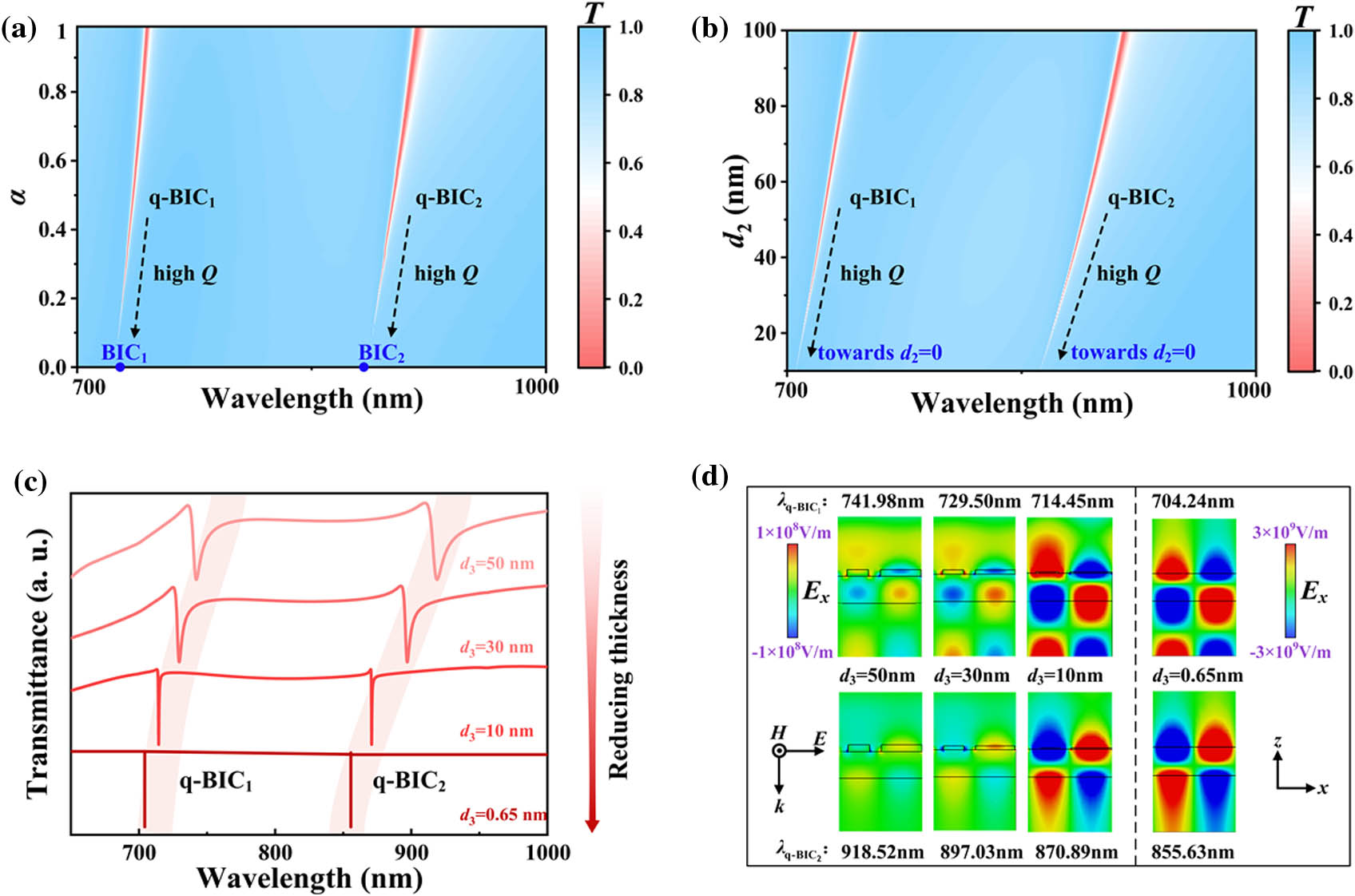
    Fig. 2. (a) Transmittance of Si metasurface with in-plane asymmetric q-BIC as a function of α, where d1=100  nm. (b) Transmittance of Si metasurface with in-plane asymmetric q-BIC as a function of d2, where α=0.9. (c) Transmittance of metasurface as a function of MoS2 thickness d3, where α=0.9. (d) Electric field distributions of metasurfaces for different MoS2 thicknesses at the resonance wavelengths of q-BIC1. For all the figures, p=560  nm.
    (a), (b) Transmittance spectra of monolayer MoS2 metasurface as α changes from 0 to 0.9 for (a) q-BIC1 and (b) q-BIC2. (c), (d) Q-factor and FWHM as functions of α for (c) q-BIC1 and (d) q-BIC2.
    Fig. 3. (a), (b) Transmittance spectra of monolayer MoS2 metasurface as α changes from 0 to 0.9 for (a) q-BIC1 and (b) q-BIC2. (c), (d) Q-factor and FWHM as functions of α for (c) q-BIC1 and (d) q-BIC2.
    (a) Resonance behavior of q-BIC1 and q-BIC2 as incident angle θ changes from 4° to 17°. (b) Q-factors of q-BIC1 and q-BIC2 with the change of θ. (c) Transmittance spectra and the corresponding electric field distributions for four incident angles of 6°, 10.4°, 10.5°, and 15°, respectively.
    Fig. 4. (a) Resonance behavior of q-BIC1 and q-BIC2 as incident angle θ changes from 4° to 17°. (b) Q-factors of q-BIC1 and q-BIC2 with the change of θ. (c) Transmittance spectra and the corresponding electric field distributions for four incident angles of 6°, 10.4°, 10.5°, and 15°, respectively.
    SHG response and enhancement factor for monolayer MoS2 metasurface and sheet Si (10 nm thick) metasurface with monolayer MoS2. Inset (I) denotes the average electric field enhancement factors for various modes. Inset (II) represents the power dependence of SHG in logarithmic scale. Here α is fixed at 0.9.
    Fig. 5. SHG response and enhancement factor for monolayer MoS2 metasurface and sheet Si (10 nm thick) metasurface with monolayer MoS2. Inset (I) denotes the average electric field enhancement factors for various modes. Inset (II) represents the power dependence of SHG in logarithmic scale. Here α is fixed at 0.9.
    Fabrication process flow of asymmetry pair of monolayer MoS2 metasurface.
    Fig. 6. Fabrication process flow of asymmetry pair of monolayer MoS2 metasurface.
    Real and imaginary parts of the refractive index for (a) Si, (b) bulk MoS2, and (c) monolayer MoS2.
    Fig. 7. Real and imaginary parts of the refractive index for (a) Si, (b) bulk MoS2, and (c) monolayer MoS2.
    Dependence of the Q-factor for the two q-BIC modes on the asymmetry parameter α and the asymmetry pair thickness d2. (a), (c) q-BIC1. (b), (d) q-BIC2.
    Fig. 8. Dependence of the Q-factor for the two q-BIC modes on the asymmetry parameter α and the asymmetry pair thickness d2. (a), (c) q-BIC1. (b), (d) q-BIC2.
    No.I0[GW/cm2]|χ(2)|max[pm/V]SHG Enhancement FactorSHG Conversion Efficiency [%]StructuresRefs.
    10.5275×10⁴z-cut LiNbO3 thin film[51]
    22.05254.2×104LiNbO3 GMR pattern[52]
    32.4683×10²LiNbO3 membrane[37]
    40.0012005×10³Si with monolayer MoS2[53]
    511700108Bulk MoS2 nanoresonators[33]
    67.280565Two multilayer GaSe on top of SiO2/Si substrate[54]
    70.001150>1095.8Asymmetry pair of monolayerMoS2This work
    Table 1. Existing SHG Conversion Efficiency on the Different Structures
    Yinong Xie, Qianting Chen, Jin Yao, Xueying Liu, Zhaogang Dong, Jinfeng Zhu. Dielectric metasurface evolution from bulk to monolayer by strong coupling of quasi-BICs for second harmonic boosting[J]. Photonics Research, 2024, 12(4): 784
    Download Citation