Double-layer high-contrast subwavelength gratings that are separated by a dielectric space layer are investigated to achieve ultra-broadband reflection. The reflection phase of subwavelength gratings and the propagation phase shift between two gratings are manipulated to expand reflection bandwidth by properly stacking two reflective gratings. A reflector exhibiting a 99% reflectance bandwidth of ~ in the near-infrared is designed. Then this reflector is prepared using laser interference lithography and ion beam planarization, and an ultra-broadband reflection is achieved with reflectance exceeding 97% over a wavelength range of 955 nm in the near-infrared region.
1. INTRODUCTION
Broadband reflectors are vital devices for many processes, such as lasers, photo detectors, and numerous other applications [1–3]. Broadband mirrors that are made with metals are widely used, but there are significant optical losses due to the presence of the imaginary part of the refractive index. Typically, distributed Bragg reflectors, also called one-dimensional photonic crystals (PCs), are used for high-reflection mirrors [4]. Such coatings have multiple layers that require precise vacuum deposition methods to control the error of coating thickness, and it is difficult to achieve broadband high reflection at infrared wavelengths due to the large coating thickness and stress [5]. Similarly, using 2D/3D PCs also can realize broadband reflection; however, the reflectors’ spatial structure is more complex and difficult to fabricate [6].
There is another more compact device, the subwavelength grating (SWG), that can achieve broadband reflection. The first experimental demonstration using an SWG including a low-index sublayer realized broadband reflection around a wavelength of 1550 nm (, ) [7]. Since the period of the SWG is shorter than the wavelength of incident light, only zeroth-order diffraction light can propagate to the far field, while other high-order diffraction light exists in the form of evanescent waves. So it is possible to concentrate almost all the energy of the incident light on the zeroth-order reflection light using the SWG [8]. This phenomenon was then explained as the interference of the internal propagation modes at the input plane and output plane [9]. It can also be interpreted as leaky-mode resonance [10]. Such gratings are called high-contrast gratings because of the high contrast of the refractive indices of the gratings and the surrounding material. Later, various single-layer SWG structures were proposed to expand reflection bandwidth, such as zero-contrast gratings [11], gratings with quasi-equilateral triangle profiles [12], and gratings with a multi-subpart profile [13].
However, the reflection bandwidth of a single-layer grating was still limited. Then the concept of multilayer gratings was proposed to broaden the reflection bandwidth. Kroker et al. reported a stacked high-contrast grating reflector with highly angular tolerant reflectance [14]. Shokooh-Saremi and Magnusson theoretically investigated an ultrawide reflector enabled with multilevel resonant leaky-mode gratings whose near field evanescent waves couple with each other, but this device is challenging in practical fabrication [15]. Niraula and Magnusson proposed multicomponent serial gratings on which zeroth-order reflected light was incoherently superimposed [16], and demonstrated experimentally that the serial gratings can provide fractional bandwidth with reflectance exceeding 98% [17]. However, this embodiment needs to package several separate SWG components together; it is not compact.
Sign up for Photonics Research TOC. Get the latest issue of Photonics Research delivered right to you!Sign up now
Here we report an ultra-broadband reflector with the structure of a double-layer SWG including a middle planarization layer. The design of this structure is inspired by the superposition of high-reflection coating stacks with different central wavelengths. A formula for the spectral transmittance of this structure based on the diffraction efficiency of each grating is provided. An ultra-broadband reflector with a reflectance of more than 99% in a wavelength range of 1307–2386 nm is designed. The experimental results are also presented; the reflector achieved possesses a reflectance of more than 97% in a wavelength range of 1467–2422 nm. This reflector is a compact device, and is straightforward to fabricate with the existing process of coating and an SWG.
2. DOUBLE-LAYER GRATING MODEL
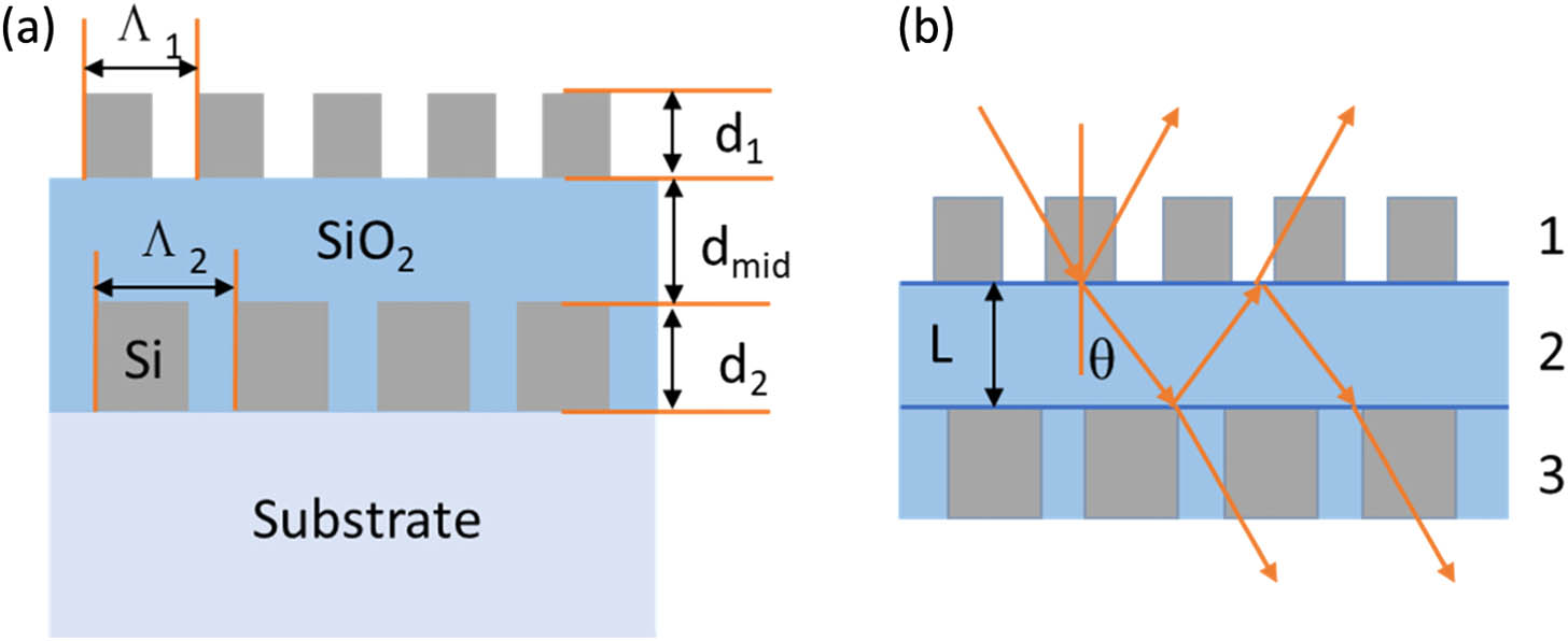
The double-layer SWG described in this paper is composed of two layers of one-dimensional silicon () grating superimposed on a fused silica substrate (), and the middle layer is a planarization layer of thin film, as shown in Fig. 1(a). The geometric parameters of the grating are as follows: period , fill factor , height of the top grating, period , fill factor , height of the bottom grating, and thickness of the planarization layer .
Figure 1.(a) Cross-sectional view of the double-layer subwavelength grating mirror, (b) interference of light between the two subwavelength gratings.
The broadband reflector is based on the overlap of the reflection bands of the two SWG reflectors, which works like two multilayer high-reflection coatings. In order to avoid high-order diffraction, each grating period is smaller than the incident wavelength. To obtain a broadband reflector, the period of the top grating must be smaller than that of the bottom grating. In other words, the top grating reflects light at shorter wavelengths, while the bottom grating reflects light at longer wavelengths. Otherwise, the light of a short wavelength will be diffracted by the top grating into multiple orders of diffracted light.
The thickness of the middle planarization layer needs to be greater than a certain value to avoid coupling of the inter-grating evanescent field, which would destroy the high-efficiency reflection of the structure [15]. In this situation, the diffractions of the two gratings are both located in their respective subwavelength regions. This structure can be abstracted as a cavity structure, as shown in Fig. 1(b), which is similar to a Fabry–Perot cavity; then the transmittance of the asymmetric cavity is given by [18] In Eq. (1), and are the transmittance and reflectivity of the interface between medium and medium , and is the round-trip phase of the cavity, given by where , and refer to the refractive index of the planarization layer, the cavity length, the angle of refraction, and the reflective phase of the single-layer SWG. From the equation, it is obvious that when the reflectivities of the two gratings are close, must not be close to 0 or ; otherwise, there will be a transmission peak similar to that in the Fabry–Perot cavity.
The reflection and transmission coefficients of each grating are calculated by rigorous coupled-wave analysis (RCWA), and the geometrical parameters of the double-layer grating are optimized by the particle swarm optimization (PSO) method. Here we will focus on the double-layer gratings to support high-efficiency broadband reflection for transverse-magnetic (TM)-polarized light at normal incidence, but the design rules apply equally well to transverse-electric (TE)-polarized light.
The PSO-optimized geometrical parameters are , , , , , and , and the thickness of the planarization layer is 1000 nm. The corresponding reflection spectrum for this double-layer grating reflector with these geometrical parameters is shown in Fig. 2. It demonstrates that the wavelength range with a reflectance higher than 99% of normally incident TM-polarized light is 1307–2386 nm, with a relative bandwidth of 58.1%. That is the broadest reflection band ever achieved by the SWG to the best of our knowledge.
Figure 2.(a) Computed zeroth-order reflectance of the two gratings for TM-polarized light at normal incidence (, and ), (b) round-trip phase of the cavity [].
Simulated zeroth-order reflectance () spectra for the two single-layer grating reflectors with these geometrical parameters are also shown in Fig. 2(a). The spectral responses are the 500 nm wide band of the top grating from 1310 to 1810 nm and the 420 nm wide band of the bottom grating from 1950 to 2370 nm, both with exceeding 99%. Therefore, this illustrates clearly that the broadband reflector is based on the overlap of the reflection bands of the two SWG reflectors.
There are some reflection dips in the operating wavelength band, which are correlated to the wavelengths where the phase is an integral multiple of , and that shows good correspondence to the Fabry–Perot interference theory. At wavelengths of about 1600 and 1900 nm, the reflectivities of the two gratings are close to each other; however, the high reflectance is still achieved due to the optimized planarization layer thickness, which enables the interference phase to avoid an integral multiple of .
3. FABRICATION, MEASUREMENT RESULTS, AND DISCUSSION
The double-layer grating device is produced in three steps. First, a thick amorphous silicon (a-Si) film with a thickness of 814 nm is deposited by magnetron sputtering on a quartz substrate. Laser interference lithography is used to expose a negative photoresist (PR), creating a grating mask. We use reactive ion etching (RIE) through the a-Si layer using an gas mixture, and remove the residual PR after RIE. Then the coating is deposited on the grating to form a planarization layer via a planarization process based on the ion beam sputtering system. This planarization technology combines ion beam etching with the coating deposition process, and has been proven effective in eliminating the influence of nodules on the scattering and the laser damage resistance of near-infrared coatings [19,20]. The coating deposition process is very reliable, and if we calibrate the etching rate carefully, the thickness of the planarization layer could be well controlled. In this paper, the deposition-etching cycle is the same as in Ref. [20]; that is, a 50 nm thick layer is deposited first, and then etched with a thickness of . This cycle is repeated 72 times to produce a planarization layer with a thickness of . Then the second layer grating is produced with the same fabrication process as the bottom grating.
Since the device is composed of a-Si with an extinction coefficient of in the operating wavelength range [21], and the SWG is scattering-free in good approximation, we can characterize the reflectance spectra as with a reasonable approximation. The zeroth-order transmittance was measured by a Cary7000 spectrometer, and the reflectance spectra are shown in Fig. 3. Comparing the measured and design spectra, it is obvious that there is low reflectance around the wavelength of 1300 nm, and this is the main factor that narrows the bandwidth of the reflector. Nevertheless, the double-layer SWG exhibits TM reflectance of in the spectral range of 1467–2422 nm, with a relative bandwidth of 49.1%. Meanwhile, the angular performance is also shown in Fig. 3, and this illustrates that the double-layer grating possesses very broadband high reflection within an angle range of 3 deg, which indicates the reflector has good tolerance of the incident angle.
Figure 3.Calculated and measured spectra of the double-layer SWG for TM-polarized light.
We also characterize the fabricated devices using scanning electron microscopy (SEM). Figure 4 displays SEM images of the fabricated grating. As seen in the cross-sectional view in the SEM image, the experimental grating parameters for the bottom grating are estimated as , , and , which are almost the same as the design values. The thickness of the planarization layer is 937 nm; this varies a little compared to the design parameter, and it results in a reflection dip around the wavelength of 1900 nm. The experimental grating parameters for the top grating are estimated as , , and , which shows that the fill factor has a large deviation compared to the design factor of 0.72, and this has significant influence on the reflection band of the double grating reflector. However, it is rather difficult to fabricate the grating with a large fill factor.
Figure 4.SEM top and cross-sectional views of the double-layer SWG on a quartz substrate.
Despite this structural deviation from the designed grating configuration, the fabricated grating exhibits a reflectance of for a bandwidth up to 950 nm. We perform an RCWA simulation with the measured structure parameters on the actual fabricated device. The calculated curve is presented in Fig. 5 and shows good agreement with the measured , clearly indicating that the fill factor of the upper grating is responsible for the narrowness of the reflection bandwidth. Therefore, by choosing a moderate fill factor for the upper grating, it is possible to improve the bandwidth of the reflectance experimentally.
Figure 5.Fitted and measured spectra of the double-layer SWG for TM-polarized light.
In summary, we have proposed and realized a double-layer SWG reflector with ultra-wideband high reflectance in TM polarization. Experimentally a reflectance of more than 97% for the wavelength range of 1467–2422 nm is demonstrated. In comparison to other stacked SWGs, the double-layer grating device is more compact, easier to fabricate, and can provide enhanced performance. Our design and experimental results will be useful for understanding the interference among multi-layer SWGs and promoting the development of stacked SWGs. Furthermore, the presence of a second SWG provides additional degrees of freedom to design spectral, angular, and polarization properties of broadband mirrors, filters, or polarizers.
[21] S. Bruynooghe, N. Schmidt, M. Sundermann, H. W. Becker, S. Spinzig. Optical and structural properties of amorphous silicon coatings deposited by magnetron sputtering. Optical Interference Coatings, ThA9(2010).