
Lei Wang, Zixian Wei, Chien-Ju Chen, Lai Wang, H. Y. Fu, Li Zhang, Kai-Chia Chen, Meng-Chyi Wu, Yuhan Dong, Zhibiao Hao, Yi Luo, "1.3 GHz E-O bandwidth GaN-based micro-LED for multi-gigabit visible light communication," Photonics Res. 9, 792 (2021)
- Photonics Research
- Vol. 9, Issue 5, 792 (2021)
Abstract
1. INTRODUCTION
Visible light communication (VLC) is a promising solution for the next-generation high-speed access technology. As an important supplement to radio frequency (RF) communication, the available spectrum of VLC is over 3 orders of magnitude wider than the RF one. VLC can be combined with solid-state lighting, which has been widely implemented in many fields. In addition, VLC exhibits the advantages of low power consumption, no electromagnetic interference, eye-safety, and strong confidentiality [1]. It is simultaneously suitable for high-speed communication and illumination applications in special environments such as airports, hospitals, nuclear power plants, underwater [2], and deep space [3]. The electrical-to-optical (E-O) bandwidth of the light-emitting device is critical in a bandwidth-limited VLC system, although there are alternative approaches to optimize the responsivity and detectivity of photodetectors such as germanium/perovskite heterostructures and InGaN multiple quantum well (QW) micro-size photodetectors [4,5]. In comparison with commercial light-emitting diodes (LEDs), micro-size LEDs (micro-LEDs) based on III-nitride semiconductors with smaller active area and lower RC delay provide a promising approach to improve the E-O bandwidth [6,7]. Beneficial from the high E-O bandwidth, the micro-LED has great potential for high-speed VLC implementation [8,9]. The data rate of micro-LED-based VLC using non-return-to-zero on-off keying (NRZ-OOK) can reach up to 1 Gbps, and multi-Gbps data rates can be achieved by advanced modulation formats such as quadrature phase shift keying (QPSK), quadrature amplitude modulation (QAM), or orthogonal frequency-division multiplexing (OFDM) [10–17]. Tsonev
However, traditional c-plane InGaN-based QW LED devices have long suffered from the limitation of the polarization-field-induced quantum-confined Stark effect (QCSE) [18]. The QCSE leads to a longer carrier lifetime in the QW at low current density, which limits the E-O bandwidth of devices. Therefore, high carrier concentration is required to screen the polarization field and shorten the carrier lifetime. A high E-O bandwidth of near 1 GHz has already been presented in micro-LEDs operating at a high current density [12,19]. However, the high current density will sacrifice the luminous efficiency of the LED which is well known as efficiency droop. Although there have been efforts to develop LED epitaxial structures optimized for shortening carrier lifetime under lower current density, the typical E-O bandwidth and operating current density of a c-plane micro-LED are still below 1 GHz and beyond
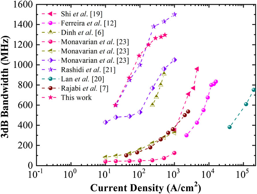
Figure 1.E-O bandwidths versus current densities for the non-polar LED, semi-polar LED, and polar LED comparison between different reports.
In this paper, we present a 1-GHz modulation bandwidth VLC system based on a single-pixel micro-LED with an E-O bandwidth of 1.3 GHz under a current density of
Sign up for Photonics Research TOC. Get the latest issue of Photonics Research delivered right to you!Sign up now
2. MATERIALS, DEVICES, AND SYSTEM SETUP
A. Epitaxial Growth
![]()
Figure 2.(a) Schematic of the epitaxial structure of the wetting layer LED. (b) A 10 μm × 10 μm AFM image of the bare wetting layer sample. (c) A 1.5 μm × 1.5 μm AFM image of the nano-structured wetting layer. (d) A high-angle annular dark field scanning transmission electron microscope (HAADF STEM) image of the LED sample. (e) A magnified bright-field (BF) STEM image of the wetting layer region.
In order to observe the morphology of the QDs and wetting layer, another sample without capping layer was grown, which maintained the same structure beneath the active region. The surface morphology of the sample was measured by a Bruker Dimension Icon atomic force microscope (AFM).
A 10 μm × 10 μm AFM image of the sample is shown as Fig. 2(b). In previous work, green InGaN QDs with a density around
In order to observe the morphology of the wetting layer sample in depth, a 1.5 μm × 1.5 μm AFM image is shown in Fig. 2(c). It can be seen that the nano-structured InGaN wetting layer appears like a broken nano-carpet. This unique nanostructure allows the wetting layer to fully release the compressive strain, thereby suppressing the QCSE and shortening the carrier life in the wetting layer. Figure 2(d) shows a high-angle annular dark-field scanning transmission electron microscope (STEM) image of the LED sample, which demonstrates that the actual thickness of each layer of the sample is quite consistent with the design. A larger magnification bright-field STEM image shows that the wetting layer has a height around 2 nm, as shown in Fig. 2(e).
B. Structure, Fabrication, Optical and Electrical Characteristics of Micro-LED
![]()
Figure 3.(a) 3D view of the designed cross-sectional structure for the micro-LED. (b) The image of the top view of the mesa/anode (75 μm/100 μm in diameter) for the micro-LED observed by scanning electron microscopy (SEM, JSM-7000F).
![]()
Figure 4.(a) Light-current density-voltage (
C. VLC System Setup
![]()
Figure 5.Schematic of the micro-LED-based VLC system in a typical indoor environment over 3-m link.
![]()
Figure 6.(a) Photograph of the micro-LED-based VLC system in a typical indoor environment. (b) Wetting layer micro-LED-based transmitter and (c) APD module-based receiver.
The QPSK-OFDM experimental demonstration can be divided into real-time communication and off-line processing. The signal is modulated and demodulated off-line, as shown in Fig. 5. First, the NRZ-OOK data stream is generated and mapped into the QPSK-OFDM signal format with 256 carriers via a MATLAB program. The modulated serial signal is converted into parallel and then Hermitian symmetry is imposed before performing an inverse fast Fourier transform. The cyclic prefix (CP) of 1/16 is inserted into the low-speed parallel blocks which are then converted back into a serial format. In addition, in order to obtain a suitable format for demodulation, a synchronization sequence is added in front of the frame, which is then uploaded into an arbitrary waveform generator (AWG, AWG7000A, Tektronix). The AWG generates an up-sampled RF signal to conduct the real-time communication experiments. At the receiver, a high-speed sampling oscilloscope (DPO75902SX, Tektronix) is used for recording the down-sampled signal with different data rates under various injection current densities. Meanwhile, a signal analyzer (N9030B, Keysight) is used to observe the signal spectrum. Recorded data have been further processed in MATLAB. After synchronization, the high-speed serial data stream is converted into low-speed parallel data blocks and the CP has been removed. Parallel time-domain signals are transformed into frequency-domain signals by a fast Fourier transform. After further performing equalization through channel estimation, the serial QAM signal is de-mapped into a baseband signal that has been then compared with the original input signal to evaluate the BER.
3. RESULTS AND DISCUSSION
A. Optical Properties and Carrier Dynamics
![]()
Figure 7.(a) TDPL spectra of the sample. The inset is a photograph of the sample excited by the laser. (b) The temperature dependence of peak wavelength and FWHM. (c) TRPL measurement. (d) Calculated
Temperature-dependent time-resolved photoluminescence (TRPL) measurement is carried out to reveal the carrier dynamics of the LED sample, and the detection wavelength is set according to the emission peak. The TRPL is performed using a tunable femtosecond laser with a 380-nm excitation wavelength and 100-fs FWHM pulse width. The repetition rate and average energy of each pulse are recorded to be 8 MHz and 62.5 pJ, respectively. Figure 7(c) shows the temperature-dependent TRPL results, which show that as the temperature increases, the carrier lifetime of the sample does not change much at first, but when the temperature exceeds 150 K the carrier lifetime begins to increase. Furthermore, TRPL curves can be fitted using a bi-exponential decay model, which is defined as follows:
B. E-O Bandwidth of Micro-LED Measured on Wafer
![]()
Figure 8.(a) E-O bandwidth of the wetting layer micro-LED on wafer measurement for different current densities. (b) Original normalized frequency response. Inset: the device under RF GS micro-probe was observed by optical microscope.
In our work, the following bandwidth measurements are strictly distinguished in different situations, which include the E-O bandwidth of the micro-LED device tested on wafer, the E-O bandwidth of the packaged micro-LED device, and the modulation bandwidth of the VLC system. Obviously, considering the actual application, the values of bandwidth will decrease from the micro-LED chip to the packaged micro-LED device, and then decrease from the packaged micro-LED device to the modulation bandwidth of the VLC system. Therefore, the back-to-back data transmission can obtain maximum data rate over an optical fiber. For real experimental demonstration of the VLC system, the data rate is lower than back-to-back limited by communication distance, packaging of devices, optical power, channel loss, and other factors.
The abovementioned E-O bandwidth value of 1.3 GHz for c-plane polar micro-LEDs before packaging is tested on wafer using a plastic optical fiber to export light which exhibits the LED under a radio-frequency ground-signal (RF GS) micro-probe. It is not difficult to notice that there is no communication distance in some publications, which is impossible in the real application of VLC systems [23]. Therefore, the data rate from testing on wafer by the GS micro-probe with collecting by plastic optical fiber over 0 m free-space communication distance as shown in Fig. 8(b) is totally different from a real system compared with the micro-LED-based VLC system in Fig. 6(a). The measured modulation bandwidth of 1 GHz is limited by the bandwidth of the APD receiver and influenced by the free-space channel conditions and the attenuation of the optical power, which results in the decline of bandwidth from 1.3 to 1 GHz.
C. System Communication Performances Measurement
![]()
Figure 9.(a) Normalized frequency responses of the VLC system with various current densities. (b) The extracted 3-dB modulation bandwidth and received optical power.
![]()
Figure 10.Comparison of optical power between the emitter side and the receiver side and the
![]()
Figure 11.(a) Data rates versus BER for the experimentally obtained results and the eye diagrams of (b) 1.0 Gbps, (c) 1.2 Gbps, (d) 1.4 Gbps, (e) 1.6 Gbps, (f) 1.8 Gbps, and (g) 2.0 Gbps data rates at the driving current density of
![]()
Figure 12.SNR versus data rate of the micro-LED-based VLC system using NRZ-OOK format at different current densities.
![]()
Figure 13.(a) Data rate and related BER of QPSK-OFDM at different current densities and the constellation diagrams with the data rate change of (b) 1 Gbps, (c) 2 Gbps, (d) 3 Gbps, and (e) 4 Gbps at the current density of
![]()
Figure 14.Corresponding frequency spectrograms with the data rate change from 1 to 4 Gbps at the current density of
Finally, we compare our wetting layer micro-LED-based VLC system with other point-to-point VLC systems based on single-pixeled LEDs which have been reported in other literature. As shown in Table 2, compared with the works of Islim
Performance of VLC Systems Based on Single-Pixeled Micro-LED (Summary of Part of Existing Works)
| Optical | Bandwidth | Modulation | Highest | Distance | ||||
|---|---|---|---|---|---|---|---|---|
| 2014 | [ | Blue μLED | 4.5 | 60 | mQAM-OFDM | 3 | 0.05 | |
| 2015 | [ | UV | 2.5 | 130 | mQAM-OFDM | 3.32 | – | |
| 2016 | [ | Blue μLED | 2.7 | 800 | NRZ-OOK | 1.7 | 0.5 | |
| 5.7 | PAM4 | 3.5 | 0.75 | |||||
| mQAM-OFDM | 5 | 0.75 | ||||||
| 2017 | [ | Violet μLED | 655 | mQAM-OFDM | 7.91 | |||
| 2017 | [ | μLED | 0.8 | NRZ-OOK | 1.3 | 3 | ||
| 1 | 10 | |||||||
| 0.87 | 16 | |||||||
| 2018 | [ | μLED + YQDs | 85 | NRZ-OOK | 0.3 | |||
| 2018 | [ | μLED-based detector | – | – | NRZ-OOK | 0.185 | ||
| 2019 | [ | 285 | NRZ-OOK | 2.1 | 0.3 | |||
| PAM4 | 2.55 | 0.3 | ||||||
| mQAM-OFDM | 5.18 | 0.3 | ||||||
| 2019 | [ | UV μLEDs | 0.196 | 438 | NRZ-OOK | 0.8 | 0.3 | |
| mQAM-OFDM | 1.1 | |||||||
| 2019 | [ | Dual-color μLED arrays | 0.85/1.04 | 427/134 | mQAM-OFDM | 3.35 | – | 0.3 |
| 2020 | Our work | Blue wetting layer μLED | 0.82 | 1000 | NRZ-OOK | 2 | 3 | |
| QPSK-OFDM | 4 | 3 |
μLED: micro-size LED.
QAM-OFDM: quadrature amplitude modulation-orthogonal frequency division multiplexing.
UV: ultraviolet.
NRZ-OOK: non-return-to-zero on-off-keying.
PAM4: pulse-amplitude-modulation 4-level.
YQDs: yellow quantum dots.
The emitting optical power at the current density of
QPSK-OFDM: quadrature phase shift keying-orthogonal frequency-division multiplexing.
4. CONCLUSION
In conclusion, for solving the intrinsic bandwidth limitation of luminescent devices in the VLC systems, self-assembly grown nano-structured InGaN wetting layers were adopted as the active layers of a high-speed LED. A 480-nm blue micro-LED with 1.3 GHz E-O bandwidth on c-plane GaN is presented in this paper which is much higher than any other reports based on the c-plane epitaxy. The VLC system modulation bandwidth can reach 1 GHz after using the packaged micro-LED as transmitter. In addition, to give a comprehensive evaluation, we employed the micro-LEDs in a VLC system and demonstrate a 3-m data transmission over air channel, which has the highest distance-bandwidth product of 3 GHz·m among all the point-to-point VLC systems based on a single-pixel LED. By employing a
References
[1] A. Tsiatmas, C. P. M. J. Baggen, F. M. J. Willems, J. M. G. Linnartz, J. W. M. Bergmans. An illumination perspective on visible light communications. IEEE Commun. Mag., 52, 64-71(2014).
[2] Z. Zeng, S. Fu, H. Zhang, Y. Dong, J. Cheng. A survey of underwater optical wireless communications. IEEE Commun. Surveys Tuts., 19, 204-238(2017).
[3] C. Tsai, C. Cheng, H. Kuo, G. Lin. Toward high-speed visible laser lighting based optical wireless communications. Prog. Quantum Electron., 67, 100225(2019).
[4] W. Hu, H. Cong, W. Huang, Y. Huang, L. Chen, A. Pan, C. Xue. Germanium/perovskite heterostructure for high-performance and broadband photodetector from visible to infrared telecommunication band. Light Sci. Appl., 8, 106(2019).
[5] K. Ho, R. Chen, G. Liu, C. Shen, J. Holguin-Lerma, A. A. Al-Saggaf, T. K. Ng, M. Alouini, J. He, B. S. Ooi. 3.2 gigabit-per-second visible light communication link with InGaN/GaN MQW micro-photodetector. Opt. Express, 26, 3037-3045(2018).
[6] D. V. Dinh, Z. Quan, B. Roycroft, P. J. Parbrook, B. Corbett. GHz bandwidth semipolar (112-2) InGaN/GaN light-emitting diodes. Opt. Lett., 41, 5752-5755(2016).
[7] K. Rajabi, J. Wang, J. Jin, Y. Xing, L. Wang, Y. Han, C. Sun, Z. Hao, Y. Luo, K. Qian, C. Chen, M. Wu. Improving modulation bandwidth of c-plane GaN-based light-emitting diodes by an ultra-thin quantum wells design. Opt. Express, 26, 24985-24991(2018).
[8] H. Han, H. Lin, C. Lin, W. Chong, J. Li, K. Chen, P. Yu, T. Chen, H. Chen, K. Lau, H. Kuo. Resonant-enhanced full-color emission of quantum-dot-based micro LED display technology. Opt. Express, 23, 32504-32515(2015).
[9] T. Wu, C. Sher, Y. Lin, C. Lee, S. Liang, Y. Lu, S. H. Chen, W. Guo, H. Kuo, Z. Chen. Mini-LED and micro-LED: promising candidates for the next generation display technology. Appl. Sci., 8, 1557(2018).
[10] D. Tsonev, H. Chun, S. Rajbhandari, J. J. D. McKendry, S. Videv, E. Gu, M. Haji, S. Watson, A. E. Kelly, G. Faulkner, M. D. Dawson, H. Haas, D. O’Brien. A 3-Gb/s single-LED OFDM-based wireless VLC link using a gallium nitride μLED. IEEE Photonics Technol. Lett., 26, 637-640(2014).
[11] J. J. D. McKendry, D. Tsonev, R. Ferreira, S. Videv, A. D. Griffiths, S. Watson, E. Gu, A. E. Kelly, H. Haas, M. D. Dawson. Gb/s single-LED OFDM-based VLC using violet and UV gallium nitride μLEDs. IEEE Summer Topicals Meeting Series (SUM), 175-176(2015).
[12] R. X. G. Ferreira, E. Xie, J. J. D. McKendry, S. Rajbhandari, H. Chun, G. Faulkner, S. Watson, A. E. Kelly, E. Gu, R. V. Penty, I. H. White, D. C. O. Brien, M. D. Dawson. High bandwidth GaN-based micro-LEDs for multi-Gb/s visible light communications. IEEE Photonics Technol. Lett., 28, 2023-2026(2016).
[13] M. S. Islim, R. X. Ferreira, X. He, E. Xie, S. Videv, S. Viola, S. Watson, N. Bamiedakis, R. V. Penty, I. H. White, A. E. Kelly, E. Gu, H. Haas, M. D. Dawson. Towards 10 Gb/s orthogonal frequency division multiplexing-based visible light communication using a GaN violet micro-LED. Photon. Res., 5, A35-A43(2017).
[14] C. Chen, J. Yan, D. Chen, K. Lin, K. Feng, M. Wu. A 520-nm green GaN LED with high bandwidth and low current density for gigabits OFDM data communication. Optical Fiber Communication Conference (OFC), Th2A.18(2018).
[15] X. He, E. Xie, M. S. Islim, A. A. Purwita, J. J. D. McKendry, E. Gu, H. Haas, M. D. Dawson. 1 Gbps free-space deep-ultraviolet communications based on III-nitride micro-LEDs emitting at 262 nm. Photon. Res., 7, B41-B47(2019).
[16] S. Mei, X. Liu, W. Zhang, R. Liu, L. Zheng, R. Guo, P. Tian. High-bandwidth white-light system combining a micro-LED with perovskite quantum dots for visible light communication. ACS Appl. Mater. Interface, 10, 5641-5648(2018).
[17] E. Xie, X. He, M. S. Islim, A. A. Purwita, J. J. D. McKendry, E. Gu, H. Haas, M. D. Dawson. High-speed visible light communication based on a III-nitride series-biased micro-LED array. J. Lightwave Technol., 37, 1180-1186(2019).
[18] S. Tsai, C. Lu, C. Liu. Piezoelectric effect on compensation of the quantum-confined Stark effect in InGaN/GaN multiple quantum wells based green light-emitting diodes. Nano Energy, 28, 373-379(2016).
[19] J. Shi, K. Chi, J. Wun, J. E. Bowers, Y. Shih, J. Sheu. III-nitride-based cyan light-emitting diodes with GHz bandwidth for high-speed visible light communication. IEEE Electron Device Lett., 37, 894-897(2016).
[20] H. Lan, I. Tseng, H. Kao, Y. Lin, G. Lin, C. Wu. 752-MHz modulation bandwidth of high-speed blue micro light-emitting diodes. IEEE J. Quantum Electron., 54, 3300106(2018).
[21] A. Rashidi, M. Monavarian, A. Aragon, A. Rishinaramangalam, D. Feezell. Nonpolar m-plane InGaN/GaN micro-scale light-emitting diode with 1.5 GHz modulation bandwidth. IEEE Electron Device Lett., 39, 520-523(2018).
[22] M. Monavarian, A. Rashidi, A. A. Aragon, M. Nami, S. H. Oh, S. P. DenBaars, D. Feezell. Trade-off between bandwidth and efficiency in semipolar (2021) InGaN/GaN single-and multiple-quantum-well light-emitting diodes. Appl. Phys. Lett., 112, 191102(2018).
[23] M. Monavarian, A. Rashidi, A. A. Aragon, S. H. Oh, A. K. Rishinaramangalam, S. P. DenBaars, D. Feezell. Impact of crystal orientation on the modulation bandwidth of InGaN/GaN light-emitting diodes. Appl. Phys. Lett., 112, 041104(2018).
[24] M. Haemmer, B. Roycroft, M. Akhter, D. V. Dinh, Z. Quan, J. Zhao, P. J. Parbrook, B. Corbett. Size-dependent bandwidth of semipolar (1122) light-emitting-diodes. IEEE Photonics Technol. Lett., 30, 439-442(2018).
[25] H. Gao, F. Yan, Y. Zhang, J. Li, Y. Zeng, J. Wang. Growth of nonpolar a-plane GaN on nano-patterned r-plane sapphire substrates. Appl. Surf. Sci., 255, 3664-3668(2009).
[26] L. Wang, L. Wang, J. Yu, Z. Hao, Y. Luo, C. Sun, Y. Han, B. Xiong, J. Wang, H. Li. Abnormal Stranski–Krastanov mode growth of green InGaN quantum dots: morphology, optical properties, and applications in light-emitting devices. ACS Appl. Mater. Interface, 11, 1228-1238(2019).
[27] A. Hu, H. Tian, Q. Liu, L. Wang, L. Wang, X. He, Y. Luo, X. Guo. Graphene on self-assembled InGaN quantum dots enabling ultrahighly sensitive photodetectors. Adv. Opt. Mater., 7, 1801792(2019).
[28] M. Arita, F. Le Roux, M. J. Holmes, S. Kako, Y. Arakawa. Ultraclean single photon emission from a GaN quantum dot. Nano Lett., 17, 2902-2907(2017).
[29] Z. Gačević, M. Holmes, E. Chernysheva, M. Müller, A. Torres-Pardo, P. Veit, F. Bertram, J. Christen, J. M. González Calbet, Y. Arakawa, E. Calleja, S. Lazić. Emission of linearly polarized single photons from quantum dots contained in nonpolar, semipolar, and polar sections of pencil-like InGaN/GaN nanowires. ACS Photonics, 4, 657-664(2017).
[30] D. Wang, T. Zhu, R. A. Oliver, E. L. Hu. Ultra-low-threshold InGaN/GaN quantum dot micro-ring lasers. Opt. Lett., 43, 799-802(2018).
[31] G. Weng, Y. Mei, J. Liu, W. Hofmann, L. Ying, J. Zhang, Y. Bu, Z. Li, H. Yang, B. Zhang. Low threshold continuous-wave lasing of yellow-green InGaN-QD vertical-cavity surface-emitting lasers. Opt. Express, 24, 15546-15553(2016).
[32] E. P. O. Reilly, S. Schulz. Theory of reduced built-in polarization field in nitride-based quantum dots. Phys. Rev. B, 82, 033411(2010).
[33] M. Zhang, P. Bhattacharya, W. Guo. InGaN/GaN self-organized quantum dot green light emitting diodes with reduced efficiency droop. Appl. Phys. Lett., 97, 011103(2010).
[34] L. Wang, D. Yang, Z. Hao, Y. Luo. Metal–organic–vapor phase epitaxy of InGaN quantum dots and their applications in light-emitting diodes. Chin. Phys. B, 24, 067303(2015).
[35] X. Liu, P. Tian, Z. Wei, S. Yi, Y. Huang, X. Zhou, Z.-J. Qiu, L. Hu, Z. Fang, C. Cong, L. Zheng, R. Liu. Gbps long-distance real-time visible light communications using a high-bandwidth GaN-based micro-LED. IEEE Photonics J., 9, 7204909(2017).
[36] X. Liu, R. Lin, Z. Qian, H. Chen, X. Zhou, G. Zhou, X. Cui, X. Zhou, L. Zheng, R. Liu, P. Tian. An InGaN micro-LED based photodetector array for high-speed parallel visible light communication. Asia Communications and Photonics Conference (ACP), 1-3(2018).
[37] J. F. C. Carreira, E. Xie, R. Bian, C. Chen, J. J. D. McKendry, B. Guilhabert, H. Haas, E. Gu, M. D. Dawson. On-chip GaN-based dual-color micro-LED arrays and their application in visible light communication. Opt. Express, 27, A1517-A1528(2019).


Set citation alerts for the article
Please enter your email address

© Copyright 2018-2021 | Chinese Laser Press. All Rights Reserved 沪ICP备15018463号-20