• Journal of the European Optical Society-Rapid Publications
  • Vol. 19, Issue 1, 2022017 (2023)
Junyi Yan1, Yi Li1、2、*, Mengdi Zou1, Jiaqing Zhuang1, Jincheng Mei1, Xingping Wang1, Xin Zhang1, Yuda Wu1, Chuang Peng1, Wenyan Dai1, Zhen Yuan1, and Ke Lin1
Author Affiliations
  • 1School of Optical-Electrical and Computer Engineering, University of Shanghai for Science and Technology, Shanghai 200093, China
  • 2Shanghai Key Laboratory of Modern Optical System, Shanghai 200093, China
  • show less
    DOI: 10.1051/jeos/2022017 Cite this Article
    Junyi Yan, Yi Li, Mengdi Zou, Jiaqing Zhuang, Jincheng Mei, Xingping Wang, Xin Zhang, Yuda Wu, Chuang Peng, Wenyan Dai, Zhen Yuan, Ke Lin. Ultra-broadband and tunable infrared absorber based on VO2 hybrid multi-layer nanostructure[J]. Journal of the European Optical Society-Rapid Publications, 2023, 19(1): 2022017 Copy Citation Text show less
    Schematic diagram of absorber by hybrid integration of the upper and lower parts.
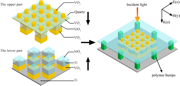
    Fig. 1. Schematic diagram of absorber by hybrid integration of the upper and lower parts.
    (a) Schematic of the unit cell of the absorber. (b) The cross-sectional view of the absorber. (c) Top view of the unit cell for the absorber.
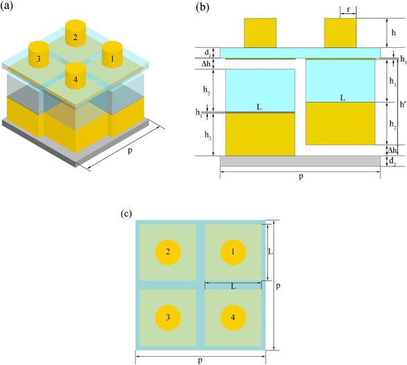
    Fig. 2. (a) Schematic of the unit cell of the absorber. (b) The cross-sectional view of the absorber. (c) Top view of the unit cell for the absorber.
    (a) Absorption change with h1. (b) Absorption change with h2. (c) Absorption change with h3. (d) Absorption change with L.
    Fig. 3. (a) Absorption change with h1. (b) Absorption change with h2. (c) Absorption change with h3. (d) Absorption change with L.
    (a) Absorption change with L when the VO2 nanocylinder array is prepared on the front illuminated surface. (b) Absorption change with the radius of the VO2 nanocylinder array r. (c) Absorption change with the height of the VO2 nanocylinder array h. (d) Absorption change with the structural spacing Δh. (e) Absorption change with the variation of individual cycle size p.
    Fig. 4. (a) Absorption change with L when the VO2 nanocylinder array is prepared on the front illuminated surface. (b) Absorption change with the radius of the VO2 nanocylinder array r. (c) Absorption change with the height of the VO2 nanocylinder array h. (d) Absorption change with the structural spacing Δh. (e) Absorption change with the variation of individual cycle size p.
    Calculated absorption spectrum.
    Fig. 5. Calculated absorption spectrum.
    (a) The electric field distribution in XY plane. (b) The magnetic field distribution in XY plane. (c) The electric field distribution in XZ plane. (d) The magnetic field distribution in XZ plane.
    Fig. 6. (a) The electric field distribution in XY plane. (b) The magnetic field distribution in XY plane. (c) The electric field distribution in XZ plane. (d) The magnetic field distribution in XZ plane.
    (a) Steady state temperature field distribution of the absorber. (b) Transient temperature change of the absorber. (c) Absorption change with alignment deviation. (d) Absorption change with T1 and T2. (e) Absorption change with ambient temperature T.
    Fig. 7. (a) Steady state temperature field distribution of the absorber. (b) Transient temperature change of the absorber. (c) Absorption change with alignment deviation. (d) Absorption change with T1 and T2. (e) Absorption change with ambient temperature T.
    Absorption spectra at different polarization angles.
    Fig. 8. Absorption spectra at different polarization angles.
    (a) Absorption spectra at different incident angles under TE. (b) Absorption spectra at different incident angles under TM.
    Fig. 9. (a) Absorption spectra at different incident angles under TE. (b) Absorption spectra at different incident angles under TM.
    WorksDevice configurationΔB (μm)ĀFOM (μm)Tuning methodh(λ) × ΔB (μm)Materials involvedMaximum incidence angle
    [29]MIM tri-layer0.4–2 (1.6)91.4%0.82N/AN/ATi, SiO2, Ti50°
    [14]MIM tri-layer0.1–1.9 (1.8)93.2%1.67N/AN/ATi, W, SiO2, Au45°
    [43]Planar layered thin film structures2–5 (3)85.3%2.55Thermal1.8Sapphire, VO2, PMMA, Au60°
    [44]L-shaped hybrid nanostructures MIM tri-layer4.5–6.5 (2)92.4%1.84Thermal1.54Au, VO2, AuN/A
    [28]Patterned plasmonic metasurface MIM tri-layer1.6–4.7 (3.1)93.7%2.9Thermal1.92Cr, VO260°
    [45]Hybrid nanodisc array MIM tri-layer0.7–1.8 (1.1)87.6%0.96Thermal0.7Au, VO2, Au70°
    [42]Nanocolumn array2–4.8 (2.8)95.5%2.67Thermal1.4VO2, SiO2, W, Al2O350°
    Our workHybrid multi-layer nanostructure1.5–8 (6.5)94.7%6.15Thermal3.35VO2, SiO2, Ti60°
    Table 1. Comparison of works on the broadband absorbers in the NMIR range in recent years.
    Junyi Yan, Yi Li, Mengdi Zou, Jiaqing Zhuang, Jincheng Mei, Xingping Wang, Xin Zhang, Yuda Wu, Chuang Peng, Wenyan Dai, Zhen Yuan, Ke Lin. Ultra-broadband and tunable infrared absorber based on VO2 hybrid multi-layer nanostructure[J]. Journal of the European Optical Society-Rapid Publications, 2023, 19(1): 2022017
    Download Citation