
Liting Hu, Lingfei Ji, Yan Wu, Zhenyuan Lin. Preparation of p-Type Heavily-Doped 4H-SiC by Laser Irradiation of Solid Al Film[J]. Chinese Journal of Lasers, 2018, 45(6): 0603003
- Chinese Journal of Lasers
- Vol. 45, Issue 6, 0603003 (2018)
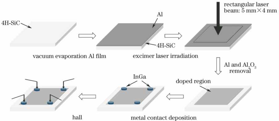
Fig. 1. Schematic of experimental procedure
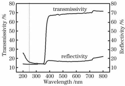
Fig. 2. Curves of transmissivity and reflectivity of 4H-SiC
Fig. 3. EDS patterns on surface of samples before and after Al doping. (a) Undoped 4H-SiC;(b) 4H-SiC with a Al film thickness of 240 nm
Fig. 4. Resistance tests. (a) Schematic; (b) I-V curves between electrodes 1 and 2;(c) I-V curve between electrodes 3 and 4
Fig. 5. Ohmic contact versus Al film thickness and number of laser pulses
Fig. 6. Optical micrographs and surface roughness of 4H-SiC under different numbers of laser pulses.(a) 1, micrograph; (b) 50, micrograph; (c) 1, roughness; (d) 50, roughness
Fig. 7. Resistivity and carrier concentration versus number of laser pulses. (a) Bulk resistivity;(b) bulk carrier concentration
Fig. 8. Hall test results of laser irradiated 4H-SiC when Al film thickness is 120 nm and number of laser pulses is 50. (a) I-V curves between electrodes 1 and 2; (b) I-V curves between electrodes 1 and 2
Fig. 9. XPS spectra on surface of 4H-SiC before and after Al doping
Fig. 10. XPS spectra on surface of 4H-SiC before and after Al doping. (a) Si 2p orbit; (b) C 1s orbit; (c) Al 2p orbit
| |||||||||||||||||||||||||||
Table 1. Surface element contents of laser irradiated 4H-SiC with a Al film thickness of 240 nm

Set citation alerts for the article
Please enter your email address
© Copyright 2018-2021 | Chinese Laser Press. All Rights Reserved 沪ICP备15018463号-20