
Haochuan Wan, Yunqi Cao, Li-Wei Lo, Zhihao Xu, Nelson Sepúlveda, Chuan Wang. Screen-printed soft triboelectric nanogenerator with porous PDMS and stretchable PEDOT:PSS electrode[J]. Journal of Semiconductors, 2019, 40(11): 112601
- Journal of Semiconductors
- Vol. 40, Issue 11, 112601 (2019)
Abstract
1. Introduction
Rapid growth in the wearable electronics market has led to tremendous amount of new scientific discoveries and technological developments recently. The flexible electronics and stretchable electronics technologies have been extensively studied for applications in flexible/stretchable display[
Among various stretchable triboelectric materials, elastomer polydimethylsiloxane (PDMS) has been widely used in wearable TENG applications due to its high electronegativity, biocompatibility and simple processing[
In this work, we demonstrate a PDMS-based TENG device with screen-printed stretchable electrode and porous PDMS thin film formed by using self-assembled polystyrene beads as the sacrificial template. The conductive polymer poly(3,4-ethylenedioxythiophene) polystyrene sulfonate (PEDOT:PSS) mixed with bis(trifluoromethane)sulfonimide lithium salt was used as the stretchable conductor and screen-printed onto the porous PDMS, which serves as both the contacting surface and as an electrode. Compared to similar TENG device made with non-porous PDMS, we have observed 2.5 times improvement in output voltage and 1.6 times improvement in output current. The scalable and low-cost fabrication process and great performance offered by the porous PDMS TENG makes it promising for a wide range of applications in wearable energy harvesting devices or sensors.
2. Experiments
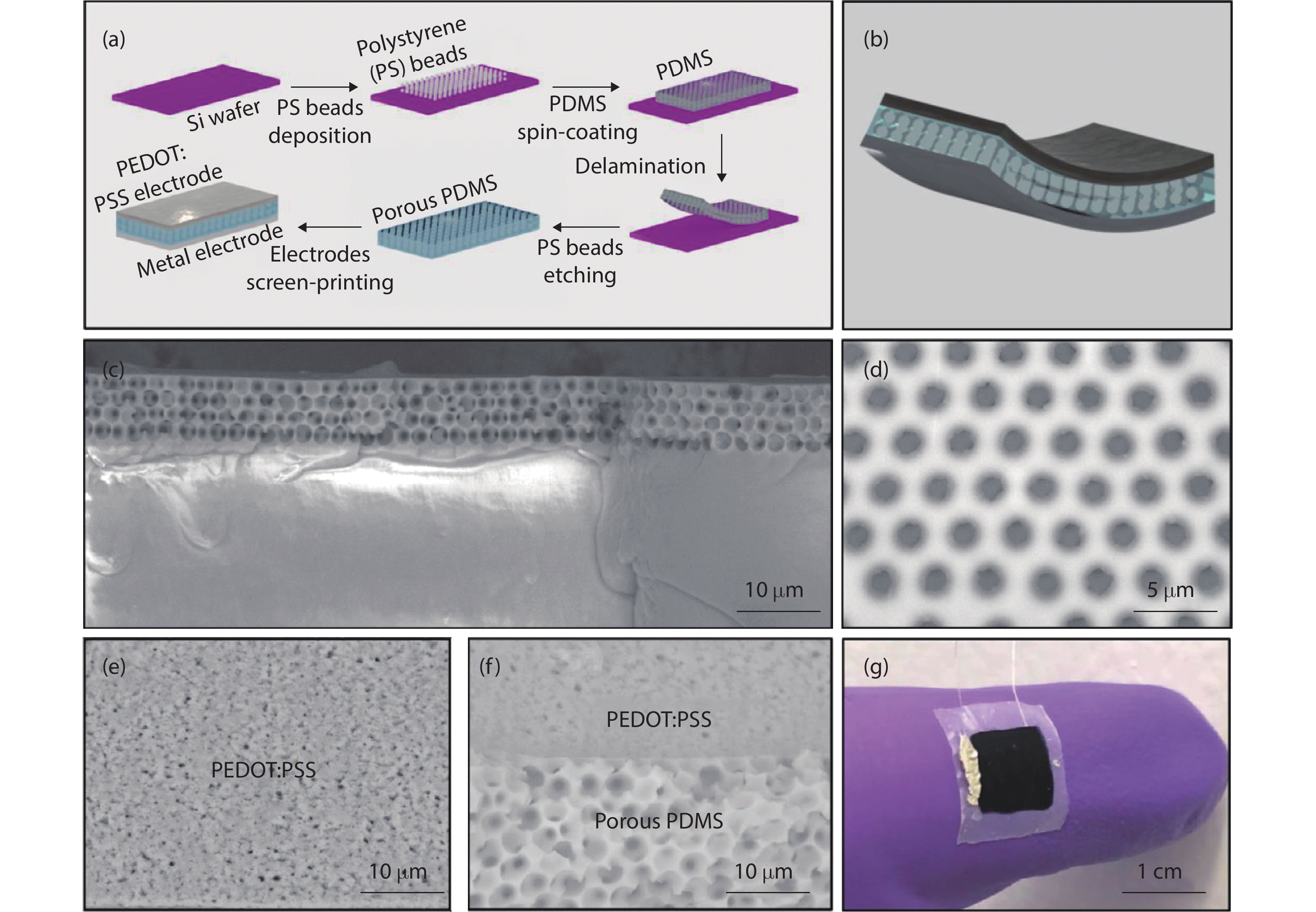
Schematic diagrams illustrating the fabrication processes and photographic images of porous PDMS TENG are illustrated in Figs. 1(a), 1(b) and 1(g). 50 μL of polystyrene (PS) latex microspheres water dispersion (6 μm, 2.5 wt%, Alfa Aesar) was drop-casted on Si substrate (1.2 × 1.2 cm2), followed by heat treatment at 65 °C for 30 min to completely evaporate the solvent. A thin-layer (~100 μm) of PDMS (Dow Corning, Sylgard 184, 10 : 1) was then spin-coated (1000 rpm, 60 s) on the sample and heated on a heating plate at 80 °C for 2.5 h to cure the PDMS. After the PDMS thin film was cured, the sample was immersed in acetone briefly to detach the PS/PDMS thin film from the handling Si substrate. The fabrication of the porous PDMS thin film was completed by completely etching away the PS beads encompassed by PDMS. This was done by exposing the PS-containing side of the PDMS thin film to O2 plasma treatment (30 W, 15 s), followed by bath sonication in dimethylformamide (DMF) for 3 h and immersion in DMF at room temperature for 12 h. Figs. 1(c) and 1(d) are the cross-sectional view and top view scanning electron microscopy (SEM; JEOL, JEM-7001 LV) images of the porous PDMS thin film. The results show that highly-ordered, multilayer porous PDMS structure was successfully obtained.
![]()
Figure 1.(Color online) (a) Schematic illustration of the fabrication process of porous PDMS TENG device. (b) Schematic illustration of structure of porous PDMS TENG device. SEM images of porous PDMS thin film from (c) cross-sectional view and (d) top view. SEM images of (e) PEDOT:PSS electrode (f) PEDOT:PSS/Porous PDMS interface. (g) Photograph of fabricated porous PDMS TENG.
The composite PEDOT:PSS ink was prepared by mixing commercial PEDOT:PSS conductive screen printable ink (5 wt%, Sigma-Aldrich, Inc) with 10 wt% of bis(trifluoromethane) sulfonimide lithium salt (Sigma-Aldrich, Inc) and stirring for 15 min to further increase its stretchability[
3. Results and discussion
To confirm the template formed by PS beads has been completely etched away in the porous structure, energy dispersive X-ray analysis (EDX; JEOL, JEM-7001 LV) was conducted to the cross-sessional area of the porous PDMS structure shown in Fig. 2(a). Structural formula of PDMS and PS shown in Fig. 2(b) suggest the element content of carbon in PS (92.3 wt%) is much higher than PDMS (32.4 wt%) while the element content of silicon in PDMS is 37.8 wt% and in PS is essentially zero. EDX analysis results in Figs. 2(c) and 2(d) indicate that the voids in Fig. 2(a) have nearly zero carbon content while the silicon content is similar to the background PDMS, which suggests that all PS beads have been completely etched away in the porous PDMS structure. It is also worth noting that the fabricated porous PDMS structure remains elastic and is highly resilient to compressive strain. SEM images of the porous PDMS cross-sectional structure before (Fig. 2(f)) and after (Fig. 2(e)) pressure of up to 43.6 kPa was applied show the porous structure was fully retained after compression. The electrical property and stretchability of the screen-printed composite PEDOT:PSS electrode were also characterized. A linear stretching stage shown in Fig. 2(g) was used to apply tensile strain to a sample with PEDOT:PSS electrode, whose electrical resistance was measured under various levels of applied strain. As reported in our previous paper[
![]()
Figure 2.(Color online) (a) SEM image of porous PDMS structure examined in EDX (b) structural formula of polydimethylsiloxane (PDMS) and polystyrene (PS). Energy dispersive X-ray analysis (EDX) images of (c) carbon element and (d) silicon element of porous PDMS structure. SEM images of porous PDMS structure (e) after compressive pressure (f) before compressive pressure. (g) Photograph of the stretching test setup. (h) Resistance change of the screen-printed PEDOT:PSS electrode under various levels of applied strain.
As shown in Fig. 3, the charge generation mechanism of porous PDMS TENG device can be explained by tribo-electrification and electrostatic effect[
![]()
Figure 3.(Color online) Charge generation mechanism of the porous PDMS TENG under external compressive force.
For sandwich-structured TENG device working in contact-separation mode, the nanogenerator acts as both energy output device and energy storage device which operates similarly as a parallel-plate capacitor. The porous PDMS layer has lower elastic modulus than non-porous PDMS[
Due to the existence of both porous PDMS layer and non-porous PDMS layer, the porous PDMS TENG could be considered as two parallel-plate capacitors in stack, where the top capacitor consists of PEDOT:PSS electrode/porous PDMS layer/non-porous PDMS surface and the bottom capacitor consists of non-porous PDMS surface/non-porous PDMS layer/metal electrode. In contrast, for the non-porous PDMS TENG, the capacitors are based only on non-porous PDMS layer. Assuming the negative charge density on non-porous PDMS surface saturates at a value of σN, those negative charges are being balanced by positive charges from both the top PEDOT:PSS electrode and the bottom metal electrode during the movements. The charge density on PEDOT:PSS electrode (σP) and metal electrode (σM) should satisfy the relation of σP + σM = σN. According to the report by He et al.[
where σP represents the charge density on the PEDOT:PSS electrode, A is the electrode surface area and RL is the electrical resistance of the load resistor. The structural difference between the porous PDMS and non-porous PDMS TENG are illustrated in Fig. 4(a). To test and compare the performance of the porous PDMS and non-porous PDMS TENG, the electromechanical properties of both devices were measured. The loading force was exerted by a rubber pistol with a contact area of 6 × 6 mm2 mounted on a horizontal-moving stepping motor that is carefully aligned with the PEDOT:PSS electrode of the nanogenerator. The nanogenerator devices were mounted on a stationary stage and a commercial force sensor (A502, Tekscan, Inc) placed behind the nanogenerator was used to precisely measure the magnitude and frequency of the applied force. Output voltage and current were both measured by a Keithley 2450 Source Meter. After the measurement, a low pass filter was applied to the output voltage and current data in MATLAB to filter out the noise. From the data presented in Figs. 4(b) and 4(c), one can see that when pressed under the same amount of loading force (100 N) and frequency (0.8 Hz), due to the larger change in charge density (ΔσP) with the porous PDMS layer, the porous PDMS TENG exhibits larger average peak output voltage and output current at 1.65 V and 0.54 nA compared to non-porous PDMS TENG with 0.66 V and 0.34 nA. Furthermore, the improvement in output voltage and current might also be attributed to the increase in frictional area due to the larger surface-area-to-volume ratio offered by the porous PDMS structure, which could lead to larger charge density change as well[
![]()
Figure 4.(Color online) (a) Schematic illustrations of porous PDMS TENG (top) and non-porous PDMS TENG (bottom). (b) Output voltage and (c) output current of porous PDMS and non-porous PDMS TENG at loading force and frequency of 100 N, 0.8 Hz.
The effect of loading force and loading frequency on the output of the TENG device has also been studied. Figs. 5(a) and 5(b) present the output voltage and current of the porous PDMS TENG under various loading force from 50 to 150 N. Lee et al. has previously reported that increasing the loading force would lead to an increase in output voltage[
![]()
Figure 5.(Color online) Loading force and frequency response of porous PDMS TENG. (a) Output voltage and (b) output current response under different loading forces at same loading frequency of 0.8 Hz. (c) Output voltage and (d) output current response under different loading frequencies at same loading force of 100 N.
4. Conclusion
In summary, we have demonstrated a porous PDMS film-based TENG device using intrinsically stretchable materials and a solution-based fabrication process. The formation of highly ordered, homogeneous porous PDMS structure has been confirmed by SEM and EDX and we have shown that the use of such porous PDMS could lead to TENG device with improved energy output (2.5 times improvement in output voltage and 1.6 times in output current) that outperforms similar device with non-porous PDMS. Its output responses to different loading force and loading frequency have also been studied to characterize the device and to explore its performance limitations for further improvements. The porous PDMS film processing method and the use of intrinsically stretchable electrode materials applied in this research might pave the way for the development of low-cost and large-area stretchable TENG for wearable electronics as self-sustained power source.
Acknowledgements
This work was partially funded by a Washington University Collaboration Initiation Grant (CIG) and a Michigan State University Foundation Strategic Partnership Grant (16-SPG-Full-3236).
References
[1] C Wang, D Hwang, Z Yu et al. User-interactive electronic skin for instantaneous pressure visualization. Nat Mater, 12, 899(2013).
[2] S G R Bade, X Shan, P T Hoang et al. Stretchable light-emitting diodes with organometal-halide-perovskite-polymer composite emitters. Adv Mater, 29, 1607053(2017).
[3] X Cao, C Lau, Y Liu et al. Fully screen-printed, large-area, and flexible active-matrix electrochromic displays using carbon nanotube thin-film transistors. ACS Nano, 10, 9816(2016).
[4] W Gao, S Emaminejad, H Y Y Nyein et al. Fully integrated wearable sensor arrays for multiplexed in situ perspiration analysis. Nature, 529, 509(2016).
[5] L Cai, S Zhang, Y Zhang et al. Direct printing for additive patterning of silver nanowires for stretchable sensor and display applications. Adv Mater Technol, 3, 1700232(2018).
[6] H Shi, M Al-Rubaiai, C M Holbrook et al. Screen-printed soft capacitive sensors for spatial mapping of both positive and negative pressures. Adv Funct Mater, 29, 1809116(2019).
[7] C M Boutry, L Beker, Y Kaizawa et al. Biodegradable and flexible arterial-pulse sensor for the wireless monitoring of blood flow. Nat Biomed Eng, 3, 47(2019).
[8] Y Kim, A Chortos, W Xu et al. A bioinspired flexible organic artificial afferent nerve. Science, 360, 998(2018).
[9] R Yang, Y Qin, L Dai et al. Power generation with laterally packaged piezoelectric fine wires. Nat Nanotechnol, 4, 34(2009).
[10] W Li, D Torres, T Wang et al. Flexible and biocompatible polypropylene ferroelectret nanogenerator (FENG): on the path toward wearable devices powered by human motion. Nano Energy, 30, 649(2016).
[11] Y Cao, J Figueroa, J Pastrana et al. Flexible ferroelectret polymer for self-powering devices and energy storage systems. ACS Appl Mater Interfaces, 11, 17400(2019).
[12] F R Fan, Z Q Tian, Z L Wang. Flexible triboelectric generator. Nano Energy, 1, 328(2012).
[13] Y Zi, H Guo, Z Wen et al. Harvesting low-frequency (< 5 Hz) irregular mechanical energy: a possible killer application of triboelectric nanogenerator. ACS Nano, 10, 4797(2016).
[14] F R Fan, W Tang, Z L Wang. Flexible nanogenerators for energy harvesting and self-powered electronics. Adv Mater, 28, 4283(2016).
[15] J Chen, H Guo, X He et al. Enhancing performance of triboelectric nanogenerator by filling high dielectric nanoparticles into sponge PDMS film. ACS Appl Mater interfaces, 8, 736(2015).
[16] Y Zhu, B Yang, J Liu et al. A flexible and biocompatible triboelectric nanogenerator with tunable internal resistance for powering wearable devices. Sci Rep, 6, 22233(2016).
[17] S Wang, L Lin, Z L Wang. Nanoscale triboelectric-effect-enabled energy conversion for sustainably powering portable electronics. Nano Lett, 12, 6339(2012).
[18] F R Fan, L Lin, G Zhu et al. Transparent triboelectric nanogenerators and self-powered pressure sensors based on micropatterned plastic films. Nano Lett, 12, 3109(2012).
[19] K Y Lee, J Chun, J H Lee et al. Hydrophobic sponge structure-based triboelectric nanogenerator. Adv Mater, 26, 5037(2014).
[20] Y Wang, C Zhu, R Pfattner et al. A highly stretchable, transparent, and conductive polymer. Sci Adv, 3, e1602076(2017).
[21] X He, X Mu, Q Wen et al. Flexible and transparent triboelectric nanogenerator based on high performance well-ordered porous PDMS dielectric film. Nano Res, 9, 3714(2016).
[22] X Chen, L Miao, H Guo et al. Waterproof and stretchable triboelectric nanogenerator for biomechanical energy harvesting and self-powered sensing. Appl Phys Lett, 112, 203902(2018).
[23] C Dagdeviren, B D Yang, Y Su et al. Conformal piezoelectric energy harvesting and storage from motions of the heart, lung, and diaphragm. Proc Natl Acad Sci, 111, 1927(2014).

Set citation alerts for the article
Please enter your email address
© Copyright 2018-2021 | Chinese Laser Press. All Rights Reserved 沪ICP备15018463号-20