Qianqian SHI, Jiang WANG, Guanghua CHENG. Preparation Technology and Application of Vanadium Dioxide Thin Films(Invited)[J]. Acta Photonica Sinica, 2022, 51(10): 1016002
Search by keywords or author
- Acta Photonica Sinica
- Vol. 51, Issue 10, 1016002 (2022)
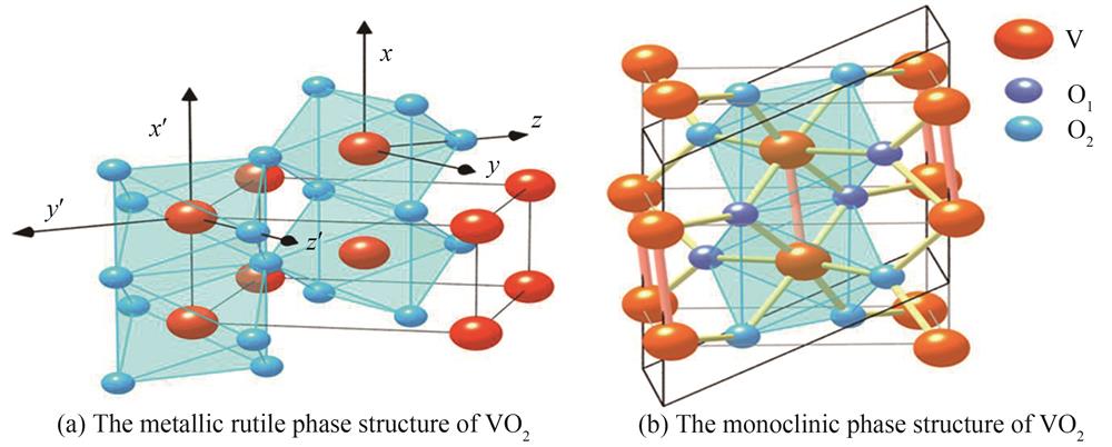
![The crystal structure of VO2[20]](/richHtml/gzxb/2022/51/10/1016002/img_01.jpg)
Fig. 1. The crystal structure of VO2[20]
![Electronic structure of VO2 monoclinic(M1)phase and rutile(R)phase[21]](/richHtml/gzxb/2022/51/10/1016002/img_02.jpg)
Fig. 2. Electronic structure of VO2 monoclinic(M1)phase and rutile(R)phase[21]
Fig. 3. Plot of the twisting angle δ vs temperature and the temperature dependence of the resistance [23]
Fig. 4. SEM images of the VO2 thin films and of HiPIMS and RFMS and their surfaces after 52 hours of ageing[37]
Fig. 5. Scheme of the hybrid process,existing of aerosol jet system(left)and laser-based curing(right)for laser direct writing[55]
Fig. 6. Schematic diagram of intelligent thermostat of VO2 and Hysteresis loops for the temperature-dependent transmittance[80,83]
Fig. 7. Experimental scheme of electrochromic intelligent window system[84]
Fig. 8. The temperature of the model house with glass and MVS[85]
Fig. 9. Schematic diagram of the hybrid VO2 cross metasurfaces[87]
Fig. 10. Simulated results of surface electric field distribution corresponding to the resonant frequency of the proposed hybrid VO2 metasurface resonator for TM mode[87]
Fig. 11. Adjustable terahertz absorber with multiple defects [89]
Fig. 12. Schematic diagram of Novel optical switch[92]
Fig. 13. Schematic and SEM images of broadband THz switch[93]
Fig. 14. Comparison of CV response of VO2 electrodes [96]
Fig. 15. Cycling performance of AC//VO2(A)@C ASC device collected at a scan rate of 50 mVs-1 for 1 000 cycles in 0.5 mol/L Na2SO4 aqueous electrolyte and LiCl/PVA gel electrolyte[18]
Fig. 16. Schematic diagrams of the experimental setups to measure temperature and pressure responses of two oscillation waveform parameters(i.e.,fo and Ao)of the Voltage-induced oscillation[100]
Fig. 17. Infrared images of the sample(diameter=1 cm)under different temperatures[102]

Set citation alerts for the article
Please enter your email address


