
Fei Hu, Li Wu, Xiyuan Dai, Shuai Li, Ming Lu, Jian Sun. Achieving high-responsivity near-infrared detection at room temperature by nano-Schottky junction arrays via a black silicon/platinum contact approach[J]. Photonics Research, 2021, 9(7): 1324
- Photonics Research
- Vol. 9, Issue 7, 1324 (2021)
Abstract
1. INTRODUCTION
A sub-bandgap near-infrared (NIR) silicon (Si) photodetector (PD) that works at room temperature (RT) can be a key component in integrated Si photonics for tele- and data communication for its good compatibility with the current complementary metal oxide semiconductor (CMOS) process flow [1–3]. It can also be used in cost-effective thermal detection and thermal imaging as focal plane arrays [4]. Multiple approaches have been proposed to enhance the NIR photo-absorption and photon-generated charge transport to improve the performance of NIR Si PDs for practical use, such as Fabry–Perot cavity design [5], waveguide configuration [6], and plasmonic enhancement [7,8]. Nonetheless, novel and facile approaches are still in demand for high-efficiency sub-bandgap NIR Si photodetection. Black Si (b-Si), i.e., Si that has been highly textured at the surface, enables strong anti-reflection via light trapping. Juntunen
2. EXPERIMENTS
Single crystalline Si (100) wafers (p-type, double-side polished, in size, ) were used as the PD substrate. The Si wafer was degreased in acetone and then ultrasonically cleaned in ethanol and deionized water successively. Next, 3 nm thick Ag layers were evaporated onto both sides of the Si wafer by resistance heating in a vacuum chamber with a base pressure lower than . After immersing the Si wafer in a solution of in volume ratio for 330 s at RT, b-Si was formed on both sides of the Si wafer via a chemical etching process catalyzed by Ag. The back side of the b-Si was deposited with a 20 nm thick Pt layer by means of magnetron sputtering. Thermal annealing in nitrogen at 950°C for 30 min was conducted to form a Si/PtSi nano-Schottky junction. The samples were also thermally annealed at 500°C, 650°C, 800°C, and 1100°C to optimize NIR absorption and detection. Before depositing the electrodes, the front surface of the sample was passivated with a 10 nm thick layer by means of e-beam evaporation, while the rear surface was passivated with a 20 nm thick one. An 80 nm thick indium-tin-oxide (ITO) layer was deposited onto the front side as the front electrode. A 2 μm thick Al layer was evaporated as the rear electrode. To enhance the electrical contact, 1 μm thick Ag grids were deposited onto the front side. Thermal annealing at 480°C in nitrogen for 5 min was conducted to anneal the passivation layers of and and form ohmic contact with the electrode. Figure 1 shows a schematic of the fabrication flow of Si PD, including preparation steps of b-Si, Schottky junction, passivation, and electrodes as described above.
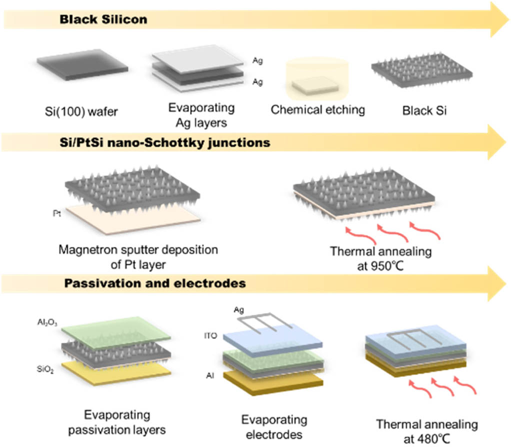
Figure 1.Schematic of fabrication flow of Si PD.
The absorption spectra were measured using an NIR spectrometer (Ideaoptics, NIR2500) with an integrating sphere. The surface morphology and the components of Si nano-pillars were measured with scanning electron microscopy (SEM) (Philips, XL30). The phase of PtSi sample was determined by X-ray diffraction (XRD) spectroscopy (Rigaku Corporation, Ultima IV). The photoelectric responsivity of PD was measured under NIR light illumination using a source meter (Keithley, SMU2400). The sub-bandgap NIR light source was a 1550 nm laser diode (CNI laser, MIL-H-1550).
Sign up for Photonics Research TOC. Get the latest issue of Photonics Research delivered right to you!Sign up now
3. RESULTS AND DISCUSSION
Figure 2(a) shows an SEM image of surface morphology for the b-Si/Pt after annealing at 950°C in nitrogen for 30 min. The corresponding cross sectional SEM is given in Fig. 2(b). Si nano-pillars are formed as found previously [11]. The average height of Si nano-pillars reads , and the average diameter reads . The aspect ratio is around 35.2. This highly nano-structured surface enables strong light trapping via a Mie scattering-like mechanism [12], and ensures efficient absorption in both visible and NIR regimes.
![]()
Figure 2.(a) Bird’s-eye view and (b) cross-sectional SEM image of b-Si/Pt after annealing at 950°C.
Figure 3(a) shows a magnified SEM image of surface morphology for the b-Si/Pt after annealing at 950°C in nitrogen for 30 min. Figure 3(b) gives the corresponding elemental maps of Pt and Si. The elemental maps are obtained according to the EDX spectra of the sample as shown in Fig. 3(c). The maps correlate well with the surface morphology of b-Si. In Fig. 3(d), EDX depth distributions of Pt after annealing at different temperatures are given. Pt atoms are found to diffuse considerably into Si nano-pillars after annealing at 950°C. As indicated by the inset in Fig. 3(d), the depth profiles are measured by means of an EDX line scan along nano-pillars from the top to the substrate of c-Si. Since the spot of electron beam of EDX is , only the average intensity of Pt signals over several Si nano-pillars is collected. In general, the zero level of depth is taken as the point where the EDX signal starts to appear and grow during the line-scan measurement. The depth profiles so obtained are similar for different locations. At such an annealing temperature, Si/PtSi Schottky junctions are formed, as shown below, which ensures both sub-bandgap NIR absorption via an inner photoemission mechanism and efficient photon-generated carrier transport [2,13].
![]()
Figure 3.(a) Magnified SEM image of surface morphology of b-Si/Pt after annealing at 950°C; (b) elemental maps of Pt and Si; (c) EDX spectra of the sample; (d) depth distributions of Pt after annealing at different temperatures.
Figure 4(a) shows the absorption spectra for b-Si/Pt contacts after annealing at different temperatures in nitrogen for 30 min. The absorptivity () is calculated in terms of the following equation:
![]()
Figure 4.(a) Absorption spectra and (b) absorption at 1550 nm for b-Si/Pt at room temperature and after annealing at 500°C, 650°C, 800°C, 950°C, and 1100°C. (c) XRD spectra for b-Si/Pt at room temperature and after annealing at 500°C and 950°C.
Figure 4(b) gives the corresponding absorptivity at 1550 nm. The absorptivity is around 71.5% at RT, then drops with the increasing annealing temperature until around 800°C, and then rises and approaches 75% at and beyond 950°C. It is seen in Fig. 4(a) that even at a wavelength of 2000 nm, the upper limit of our spectrometer, the absorptivity can still be high. Since the cutoff absorbed wavelength mainly depends on the formed Schottky barrier height—for the PtSi/p-Si in our case, it is [14]—the PD developed here could work at wavelengths longer than 1550 nm adopted in this work. At annealing temperatures of RT and 950°C, nano-Schottky junction arrays of Si/Pt and Si/PtSi form on b-Si, respectively, for their metal/semiconductor contacts. The nano-Schottky junctions are responsible for the sub-bandgap NIR absorption in terms of the inner photoemission mechanism. However, at annealing temperatures in between, Pt will react with Si, and contaminated elements such as C and O are introduced inevitably during the sample preparation process, and the higher the annealing temperature is, the more the reaction is likely to happen [14,15], which makes the number of formed nano-Schottky junctions fewer. As a result, the NIR absorptivity is reduced with the annealing temperature until 800°C. But when the crystalline phase of metallic PtSi starts to form beyond ∼800°C on b-Si, during which the defects are expelled from the Si/Pt interface automatically [14], the number of nano-Schottky junctions starts to recover, leading to an increase in NIR absorptivity. Figure 4(c) shows the XRD spectra for b-Si/Pt contacts at RT and after annealing at 500°C and 950°C in nitrogen for 30 min. For other annealing temperatures, the XRD spectra are quite similar to that at 500°C. Only at 950°C can the PtSi phase be detected. It is known that among various Si/Pt contacts, only the Si/PtSi Schottky junction is available for both the sub-bandgap NIR absorption and photodetection due to its proper electronic structures at the interface [2,16]. At RT, when Pt does not diffuse sufficiently into the Si substrate, the Schottky junction forms. But this junction contains a large number of defects at the interface of Pt and Si, such as voids, dislocations, and contaminated elements. Therefore, although the Schottky junction facilitates the sub-bandgap NIR absorption, as shown in Fig. 4(b), the obtained photocurrent is very small, due to the high recombination rate of the interfacial defects. However, when the annealing temperature approaches the crystallization temperature of the metallic PtSi phase, the process of crystallization of PtSi itself will heal the structural defects and expel the foreign elements from the interface automatically [15]. As a result, a Schottky junction with a sharp and clean interface is formed, leading to both high sub-bandgap NIR absorption and photocurrent. It is noticed that the formation or crystallization temperature of PtSi in the case of b-Si/Pt here is obviously higher than that in the case of planar bulk Si/Pt [2]. The reason could be that due to the large difference in nucleation barrier height arising from the large difference in Gibbs free energy per volume for bulk and nanostructured semiconductors, the crystallization temperature for the nanostructured semiconductor is higher than that of the bulk one [17,18]. The following b-Si NIR PDs refer only to those designed and fabricated based on the 950°C annealed b-Si/PtSi Schottky junctions, or nano-Schottky junction arrays, unless otherwise specified.
![]()
Figure 5.(a) Schematic diagram of the b-Si NIR PD with nano-Schottky detector arrays. (b) SEM image of three spots of black Si covered by
![]()
Figure 6.
Figures 6(a) and 6(b) show the current–voltage curves for the RT and 950°C annealed b-Si/Pt junctions, respectively, measured at RT under a dark condition and 1550 nm illumination. The rectifying features indicate the formation of Schottky junctions for the two cases. As expected, the photo response of the b-Si/Pt junction at RT is rather poor compared to that of b-Si/PtSi, although their absorptivity is similar. Figure 6(c) shows the current–time curves for the b-Si NIR PD made based on the Si/PtSi nano-Schottky junction arrays under off and on states of 1550 nm illumination at a fixed bias voltage of . The small increase in dark current with time could be due to a local Joule heating effect at the contact area in the initial stage when the reverse bias was applied [24].
Table 2 gives the 1550 nm photodetection characteristics for the b-Si NIR PD made based on 950°C annealed Si/PtSi nano-Schottky junction arrays, for the reverse bias voltages of , and . The specific detectivities are derived in terms of the following equation [25]: Responsivity and Specific Detectivity of 950°C Annealed b-Si NIR PD at Biased Voltages of −1.0, −1.5, and −2.0 VBiased Voltage (V) −1.0 −1.5 −2.0 Responsivity (mA/W) 147.6 293.8 478.2 Detectivity (
It is noticed that the obtained responsivities are close to those in the visible Si photodetection, and the specific detectivities are fairly high [9]. These results indicate the availability of the Si/PtSi nano-Schottky junction arrays in RT sub-bandgap NIR photodetection, as developed in this work.
4. SUMMARY
In this work, we proposed and developed a novel RT sub-bandgap NIR Si PD, based on b-Si/PtSi Schottky junctions, or nano-Schottky junction arrays. This NIR Si PD employs the properties of light trapping by b-Si, sub-bandgap absorption by Si/PtSi Schottky junction, chemical and field-effect surface passivation of b-Si by oxide layers, and nano-Schottky junction arrays for better NIR light harvesting and detection, and makes high responsivity and detectivity of RT sub-bandgap NIR Si photodetection available. This type of NIR Si PD can be cost-effectively made in a large-scale manner, and is of potential practical application for its high performance as described herein.
References
[1] M. Casalino, G. Coppola, M. Iodice, I. Rendina, L. Sirleto. Near-infrared sub-bandgap all-silicon photodetectors: state of the art and perspectives. Sensors, 10, 10571-10600(2010).
[2] M. Casalino, G. Coppola, R. M. De La Rue, D. F. Logan. State-of-the-art all-silicon sub-bandgap photodetectors at telecom and datacom wavelengths. Laser Photon. Rev., 10, 895-921(2016).
[3] W. Diels, M. Steyaert, F. Tavernier. Schottky photodiodes in bulk CMOS for high-speed 1310/1550 nm optical receivers. IEEE J. Sel. Top. Quantum Electron., 24, 3801908(2018).
[4] M. Kimata. Development of infrared focal plane arrays. Sens. Mater., 30, 1221-1230(2018).
[5] M. Casalino, G. Coppola, M. Iodice, I. Rendina, L. Sirleto. Critically coupled silicon Fabry-Perot photodetectors based on the internal photoemission effect at 1550 nm. Opt. Express, 20, 12599-12609(2012).
[6] I. Goykhman, B. Desiatov, J. Khurgin, J. Shappir, U. Levy. Waveguide based compact silicon Schottky photodetector with enhanced responsivity in the telecom spectral band. Opt. Express, 20, 28594-28602(2012).
[7] B. Desiatov, I. Goykhman, N. Mazurski, J. Shappir, J. B. Khurgin, U. Levy. Plasmonic enhanced silicon pyramids for internal photoemission Schottky detectors in the near-infrared regime. Optica, 2, 335-338(2015).
[8] M. Alavirad, A. Olivieri, L. Roy, P. Berini. High-responsivity sub-bandgap hot-hole plasmonic Schottky detectors. Opt. Express, 24, 22544-22554(2016).
[9] M. A. Juntunen, J. Heinonen, V. Vähänissi, P. Repo, D. Valluru, H. Savin. Near-unity quantum efficiency of broadband black silicon photodiodes with an induced junction. Nat. Photonics, 10, 777-781(2016).
[10] M. Steglich, M. Zilk, A. Bingel, C. Patzig, T. Käsebier, F. Schrempel, E.-B. Kley, A. Tünnermann. A normal-incidence PtSi photoemissive detector with black silicon light-trapping. J. Appl. Phys., 114, 183102(2013).
[11] L. X. Wang, Z. Q. Zhou, H. C. Hao, M. Lu. A porous Si-emitter crystalline-Si solar cell with 18.97% efficiency. Nanotechnology, 27, 425207(2016).
[12] Z. Y. Wang, R. J. Zhang, S. Y. Wang, M. Lu, X. Chen, Y. X. Zheng, L. Y. Chen, Z. Ye, C. Z. Wang, K. M. Ho. Broadband optical absorption by tunable Mie resonances in silicon nanocone arrays. Sci. Rep., 5, 7810(2015).
[13] F. D. Shepherd, A. C. Yang. Silicon Schottky retinas for infrared imaging. International Electron Devices Meeting, 310-313(1973).
[14] S. A. Ding, Z. J. Xu. Study of the relation between interfacial reaction and formation of Schottky barriers. J. Infrared Millim. Waves, 12, 385-391(1993).
[15] S. P. Murarka. Silicides for VLSI Applications, 29-70(1983).
[16] Z. J. Qiu, Z. Zhang, M. Ostling, S. L. Zhang. A comparative study of two different schemes to dopant segregation at NiSi/Si and PtSi/Si interfaces for Schottky barrier height lowering. IEEE Trans. Electron Devices, 55, 396-403(2008).
[17] M. Zacharias, P. Streitenberger. Crystallization of amorphous superlattices in the limit of ultrathin films with oxide interfaces. Phys. Rev. B, 62, 8391-8396(2000).
[18] Y. C. Fang, W. Q. Li, L. J. Qi, L. Y. Li, Y. Y. Zhao, Z. J. Zhang, M. Lu. Photoluminescence from SiO
[19] K. Xiong, S. Lu, D. Jiang, J. Dong, H. Yang. Effective recombination velocity of textured surfaces. Appl. Phys. Lett., 96, 193107(2010).
[20] Z. Q. Zhou, L. X. Wang, W. Shi, S. L. Sun, M. Lu. A synergetic application of surface plasmon and field effect to improve Si solar cell performance. Nanotechnology, 27, 145203(2016).
[21] B. Hoex, J. Schmidt, P. Pohl, M. C. M. van de Sanden, W. M. M. Kessels. Silicon surface passivation by atomic layer deposited Al2O3. J. Appl. Phys., 104, 044903(2008).
[22] B. Hoex, J. Gielis, M. Van de Sanden, W. Kessels. On the c-Si surface passivation mechanism by the negative-charge-dielectric Al2O3. J. Appl. Phys., 104, 113703(2008).
[23] J. R. Chen, D. C. Wang, H. C. Hao, M. Lu. Achieving high brightness of silicon nanocrystal light-emitting device with a field-effect approach. Appl. Phys. Lett., 104, 061105(2014).
[24] L. Dong, S. Youkey, J. Bush, J. Jiao, V. M. Dubin, R. V. Chebiam. Effects of local Joule heating on the reduction of contact resistance between carbon nanotubes and metal electrodes. J. Appl. Phys., 101, 024320(2007).
[25] F. Verstraeten, S. Gielen, P. Verstappen, J. Kesters, E. Georgitzikis, J. Raymakers, D. Cheyns, P. Malinowski, M. Daenen, L. Lutsen, K. Vandewal, W. Maes. Near-infrared organic photodetectors based on bay-annulated indigo showing broadband absorption and high detectivities up to 1.1 μm. J. Mater. Chem. C, 6, 11645-11650(2018).

Set citation alerts for the article
Please enter your email address
© Copyright 2018-2021 | Chinese Laser Press. All Rights Reserved 沪ICP备15018463号-20