
Xingyu Chen, Hao Li, Qiaoyu Chen, Haisheng Xu, Fanxuan Xie, Zheng Li, Tianye Huang, Kai Guan, Zuowei Yin, Liang Hao, Jie Yin. Recent Progress in Laser Additive Manufacturing Using Copper‑Chromium‑ Zirconium Alloys: Formation, Microstructure, and Comprehensive Properties (Invited)[J]. Chinese Journal of Lasers, 2024, 51(4): 0402302
- Chinese Journal of Lasers
- Vol. 51, Issue 4, 0402302 (2024)
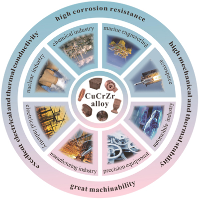
Fig. 1. Characteristics and application areas of CuCrZr alloys
![L-PBF equipment, printing principle, and prepared sample. (a) LiM-X260A L-PBF additive manufacturing equipment; (b) schematic of L-PBF printing principle[33]; (c) CuCrZr alloy sample prepared by L-PBF](/richHtml/zgjg/2024/51/4/0402302/img_02.jpg)
Fig. 2. L-PBF equipment, printing principle, and prepared sample. (a) LiM-X260A L-PBF additive manufacturing equipment; (b) schematic of L-PBF printing principle[33]; (c) CuCrZr alloy sample prepared by L-PBF
Fig. 3. Relationship between EA and density in different L-PBF experiments (the legend for samples prepared by near-infrared laser is red and the legend for samples prepared by green laser is green)
Fig. 4. Metallurgical microscopes diagrams of CuCrZr alloy samples[38]. (a) Sample with 99.15% density; (b) samples with 98.83% density; (c) sample with 98.62% density
Fig. 5. Absorptivity rate of laser by CuCrZr powder, pure Cu powder, surface-oxidized Cu powder, and Cu powder with CrZr coating (Cu@CrZr)
Fig. 6. Defects in LAM-fabricated CuCrZr samples. (a) Balling effect[39]; (b) partially melted powders[45]; (c) irregular pores[50]; (d) lack of fusion pores[16]; (e) metallurgical pores[16]; (f) crack[50]
Fig. 7. SEM images of as-built L-PBF CuCrZr sample [20]. (a)(b) Microstructure in horizontal building direction; (c)(d) microstructure in vertical building direction
Fig. 8. XRD patterns[26]. (a) CuCrZr alloy powder and L-PBF alloy; (b) 73°‒75° localized magnification
Fig. 9. Microstructure of horizontal direction of SLMed CuCrZr alloy by SEM[45]. (a)(d)(g)(j) Microstructure of AB samples; (b)(e)(h)(k) microstructure of ST samples; (c)(f)(i)(l) microstructure of SAT samples
Fig. 10. Microstructure of building direction of SLMed CuCrZr alloy by SEM[45]. (a)(d)(g)(j) Microstructure of AB samples; (b)(e)(h)(k) microstructure of ST samples; (c)(f)(i)(l) microstructure of SAT samples
Fig. 11. Thermodynamics calculation results of CuCrZr alloys using CALPHAD[29]. (a) Full range calculation results; (b) minor phases
Fig. 12. High-angle annular dark field (HAADF) analysis of DA samples[16]. (a) Aging treatment samples at 480 ℃ for 4 h; (b) aging treatment samples at 530 ℃ for 4 h; (c) aging treatment samples at 580 ℃ for 4 h
Fig. 13. TEM-EDS analysis results[16]. (a) Dispersed distribution of chromium precipitates in sample (480 ℃ aging treatment for 4 h); (b) aggregated and growing chromium and zirconium precipitates in sample (580 ℃ aging treatment for 4 h)
Fig. 14. HAADF/STEM and Cr and Zr EDX analysis results[20]. (a) No micro and nano-precipitates detected in the as-built samples; (b) Cr precipitates detected after DAH; (c) Zr precipitates appearing next to Cr precipitates after DAH; (d) substrate of pure Cu
Fig. 15. XRD patterns[25]. (a) CuCrZr samples in the as-built state and CuCrZr samples with heat treatments; (b) enlarged spectra in the 40°~45° 2θ range
Fig. 16. Mechanical behavior of L-PBF-built CuCrZr alloys[31]. (a) Stress and strain plots of samples in horizontal and vertical building directions; (b) tensile fracture surface plots in horizontal building direction; (c) tensile fracture surface plots in vertical building direction
Fig. 17. Tensile test results of samples along the build direction at room temperature, 204 ℃, and 427 ℃[57]. (a) AB sample; (b) 420 ℃ aging treatment for 2 h; (c) 500 ℃ aging treatment for 2 h; (d) 575 ℃ aging treatment for 2 h; (e) 650 ℃ aging treatment for 2 h
Fig. 18. Relationship between density and electrical conductivity[30]
Fig. 19. Effect of heat treatment on electrical conductivity. (a) Tang et al. [25] on heat treatment affecting electrical conductivity; (b) Yang et al. [16] on heat treatment affecting electrical conductivity; (c) Salvan et al. [20] on heat treatment affecting electrical conductivity
Fig. 20. Thermal and electrical properties of L-PBF-built CuCrZr alloys[31] . (a) Variation of thermal conductivity with temperature for CuCrZr samples; (b) effect of aging temperatures on thermal conductivity of samples
| |||||||||||||||||||||||
Table 1. Chemical composition of regular grades of CuCrZr alloys[27]
| |||||||||||||||||||||||||||||||||||||||||||||||||||||||||||||||
Table 2. Process parameters used for the highest density samples in each study
| ||||||||||||||||||||||||||||||||||||||||||||||||||||||||||||||||||||||||||||||||||||||||||||||||||||||||||||||||||
Table 3. Effect of heat treatment methods on mechanical properties
| ||||||||||||||||||||||||||||||||||||||||||||||||||||||||||
Table 4. Effect of heat treatment method on electrical conductivity
| ||||||||||||||||||||||||||||||||||||||||||
Table 5. Effect of heat treatment method on thermal conductivity

Set citation alerts for the article
Please enter your email address
© Copyright 2018-2021 | Chinese Laser Press. All Rights Reserved 沪ICP备15018463号-20