Abstract
The hybrid multiplexing technique reactivates optical interconnect as it offers multiple dimensions to dramatically enhance the data capacity of a single wavelength carrier. A straightforward method to realize hybrid multiplexing is to perform polarization multiplexing for mode-multiplexed signals, by utilizing a mode-transparent polarization beam splitter (MTPBS) which can process multiple modes simultaneously. However, present PBSs mainly work in the single-mode regime, and it is not easy to redesign the conventional PBS to accommodate multiple modes, due to the severe mode dispersion. Here, a novel MTPBS, which can tackle a group of modes simultaneously, is proposed and demonstrated. As a demonstration, the MTPBS supporting a total channel number of 13 is experimentally achieved, with low insertion loss and low modal/polarization cross talk. This work provides a new insight to realize hybrid multiplexing and represents a solution for high-density and large-capacity photonic integration.
1. INTRODUCTION
As Internet-driven traffic continues to increase dramatically, optical interconnect has been proposed to alleviate the communications bottleneck. The wavelength-division multiplexing (WDM) and polarization-division multiplexing (PDM) techniques, combined with the coherent reception and advanced modulation, have been used to achieve the capacity increment in single-mode optical interconnects. Recently, the mode-division multiplexing (MDM) technique has been emerging since it offers a new degree of freedom to multiplex spatial modes in a few-mode fiber or multimode integrated waveguide [1,2]. Compared with the WDM technique using multiple wavelengths, all the mode channels share the same wavelength for the MDM technique. Therefore, power consumption and cost can be effectively reduced, which is particularly attractive for large-scale photonic integration. Many efforts had been involved to achieve mode multiplexing [3–11], and the maximal mode number so far have reached 11 for single polarization. Despite that, it is still incommensurate with the significant development of the WDM technique with typical dozens of wavelength channels [12,13]. A straightforward method to increase the throughput of a single wavelength carrier is to combine MDM with PDM techniques to realize hybrid multiplexing. For this purpose, the mode or polarization multiplexer/demultiplexer should be specifically redesigned to accommodate the other dimension. One way is coupling the modes with different polarizations into the bus waveguide one by one [14,15]. The subsequent couplers must be very elaborately optimized to avoid polarization coupling. In this scenario, high mode-scalability is not easy to be realized due to severe polarization cross talk. The other way is using polarization-transparent couplers, each followed by a polarization beam splitter (PBS), to multiplex two modes with different polarizations [16]. However, one must design each coupler very elaborately to reduce the inter-modal cross talk. It is still a big challenge to achieve hybrid multiplexing.
Inspired by the cube PBS extensively implemented in free-space optics, we propose a novel integrated mode-transparent PBS (MTPBS) to realize hybrid multiplexing/demultiplexing. It splits the hybrid multiplexed signals (MDM and PDM) into dual-path single-polarization MDM signals, which can be subsequently handled by conventional mode demultiplexers individually to obtain separate data channels. Thus, the mode demultiplexer for each polarization can be optimized independently to decrease inter-modal cross talk, alleviating the design complexity greatly. Conventional PBSs based on lateral evanescent coupling [17–19] are difficult to be redesigned to realize mode-transparent manipulation, due to the severe mode dispersion. By contrast, in the proposed MTPBS, with a waveguide width much greater than wavelength, various modes tend to degenerate and behave a similar feature. In addition, being different from the conventional PBSs based on lateral evanescent coupling, the evanescent coupling in the proposed MTPBS is along the waveguide, enabling the simultaneous coupling for multiple modes. Therefore, mode-transparent operating can be fundamentally realized.
As a proof of concept, the MTPBS supporting a total channel number as high as 13, i.e., seven transverse electric (TE) mode channels and six transverse magnetic (TM) mode channels, is successfully demonstrated. For TE polarization, the insertion losses of modes are about 0.7–3.3 dB, and the modal/polarization cross talk is about . For TM polarization, the insertion losses of modes are about 1.7–3 dB, and the modal/polarization cross talk is about .
Sign up for Photonics Research TOC. Get the latest issue of Photonics Research delivered right to you!Sign up now
2. OPERATION PRINCIPLE AND SIMULATION
Figure 1(a) indicates the schematic of the proposed MTPBS adopting a bi-trench coupler. Fully etched trenches in the T-shape structure are aligned 45° with respect to the input waveguide. The light is split by the polarization state: TE polarization is reflected at 90°, while TM polarization is transmitted straightly. The incident angle is greater than the critical angle of total internal reflection (TIR) for both TE and TM polarizations, forming the TIR mirrors. A portion of input power can pass beyond the trench, provided that the trench is narrow enough [20]. The integrated MTPBS is spired by the cube PBS, which has been available commercially in free-space optics, as shown in Fig. 1(b). A pair of right-angle prisms is placed closely with each other, and a polarization-dependent dielectric coating on the hypotenuse of one prism is utilized to separate the right-angle prisms. An anti-reflection coating consisting of multilayer optical films is cemented onto each face of the cube PBS to achieve ultralow surface reflection. The cube PBS and the MTPBS possess similar geometric construction. The right-angle prism corresponds to the TIR mirror, while the dielectric coating corresponds to the trenches. The cube PBS can split arbitrarily polarized light into two orthogonal, linearly polarized components by using the polarization-dependent dielectric coating. -polarized light is turned with 90°, while -polarized light is transmitted straightly. Similarly, for the MTPBS, TE polarization can be reflected, while TM polarization is transmitted straightly.
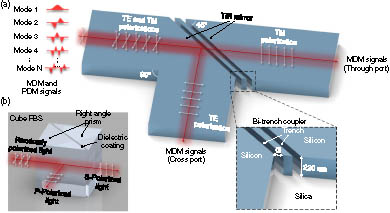
Figure 1.(a) Schematic of the MTPBS based on multimode bus waveguides which support multiple mode channels. The modes are indistinguishable, while light can be distinguished by the polarization state. Dual-polarization MDM signals can be split into TE and TM polarizations. TE MDM signals are reflected at 90°, while TM MDM signals are transmitted straightly. The bi-trench coupler consists of a pair of total internal reflection (TIR) mirrors separated by fully etched trenches. (b) Cube PBS as an analogy of MTPBS. The cube PBS consists of a pair of right-angle prisms separated by a polarization-dependent dielectric coating on the hypotenuse of one of the prisms. -polarized light is turned with 90°, while -polarized light is transmitted straightly.
To investigate the mode-transparent operation, we calculate the effective indices of eigenmodes in the waveguide with different widths, as shown in Fig. 2(a). Here, a silicon-on-insulator (SOI) platform with a 220 nm thick top silicon layer and a 2 μm thick buffer layer is adopted. The square-curves and triangle-curves correspond to TE and TM polarizations, respectively. It can be seen clearly that the mode dispersion monotonically decreases with the waveguide width. When the waveguide width is a little greater than the wavelength, the mode dispersion is significant, and the mode features are quite different, especially for the lowest- and highest-order modes. When the waveguide width is much greater than the wavelength, the modes with the same polarization tend to degenerate to the slab mode that propagates in the plane as in free space. Thus, different modes are indistinguishable and behave similar features. Note that the TE and TM polarizations cannot degenerate due to the inherent structural birefringence. Therefore, different modes with the same polarization can be tackled simultaneously, reducing the design and optimization complexity greatly. As a demonstration, we design an MTPBS supporting 13 channels, including seven TE and six TM modes. Here, the width of the bus waveguide is set as 25 μm to ensure low modal dispersion for these selected modes.

Figure 2.(a) Calculated effective indices of eigenmodes in the waveguide with different widths. The square-curves and triangle-curves are for TE and TM polarizations, respectively. (b) The simulated power transmission efficiency at through port versus different trench widths for and modes by using single-trench, bi-trench, and tri-trench couplers. The FDTD numerical method and transfer matrix theory are utilized for simulation at 1550 nm as a comparison. The trench width is the same as the gap between neighboring trenches. (c) The schematics of these three kinds of trench couplers. (d) The FDTD simulated power transmission efficiency at the through port for and modes for the bi-trench coupler at 1550 nm. The simulated mode transmission efficiency when inputting (e) , and (f) , modes from 1500 to 1600 nm. In the legend “,” the mode stands for the input mode, while the mode stands for the output mode. The letter “T” refers to the through port, and the letter “C” refers to the cross port.
The trench coupler, which previously served as a power splitter [21–23], is adopted to split polarizations here. The length of evanescent wave can be obtained approximately by [24] where is the wavenumber in free space, and is the effective refractive index of TE or TM polarization. is the refractive index of the trench, and the is the incident angle. For TM polarization, the index . For TE polarization,
The of TE or TM polarization is set as 2.847 or 2.054 at 1550 nm, and the is chosen as 45°. The lengths of the evanescent wave of TE and TM polarizations are calculated as 0.086 and 2.45 μm, respectively. It can be anticipated that TM polarization has a higher transmission efficiency than TE polarization due to stronger evanescent coupling along the waveguide. Therefore, TE and TM polarizations can be isolated by the trench coupler effectively. Note that the working mechanism of the proposed trench coupler is quite different from lateral evanescent coupling in the conventional PBS, where the strong coupling strength and low mode dispersion cannot be satisfied at the same time. To find an optimal structure to increase the TM transmission efficiency and restrict that of TE polarization, bi-trench and tri-trench couplers, which are inspired by the multilayer optical film structures of the cube PBS, are analyzed in addition to the single-trench coupler. The power transmission efficiency at the through port versus different trench widths for and modes is calculated, as shown in Fig. 2(b). Figure 2(c) illustrates the schematics of these three kinds of trench couplers. In the bi-trench and tri-trench couplers, the width of the trench equals to that of the gap between the neighboring trenches.
For the mode, the power transmission efficiency of the single-trench coupler monotonically decreases with the increase of the trench width, and the efficiency is with a trench width of 200 nm, whereas the efficiency reaches a maximum of with the trench width of 300 nm for the bi-trench coupler. The efficiency of the tri-trench coupler has two extremums of with the trench widths of 200 nm and 400 nm, respectively. For the mode, the efficiencies of the bi-trench and tri-trench couplers are much smaller compared with the single trench case. The extremum of transmission efficiency for TM polarization results from the constructive interference in the multilayer dielectric structure. We also obtain the efficiency using the transfer matrix theory applied in the multilayer dielectric structure, as the solid curves shown in Fig. 2(b). The calculated results by the transfer matrix theory agree quite well with that by the 3D finite-difference time-domain (3D FDTD) method when the trench width is small. The difference between the two methods gets more significant in the case of a wider trench width, and this can be mainly attributed to the loss induced by pinhole diffraction and Goos–Hänchen shift in the trench coupler, which are neglected by the transfer matrix theory. Although the tri-trench coupler has a high transmission efficiency around the trench widths of 200 and 400 nm, the curve of the bi-trench coupler around the extremum of 300 nm is flatter, corresponding to a larger fabrication robustness. Therefore, the bi-trench coupler with the trench width of 300 nm is adopted.
Figure 2(d) exhibits the simulated power transmission efficiency with different trench widths at the through port, for and modes, respectively. It can be seen clearly the maximal efficiency is obtained with the trench width of 300 nm for modes, and the efficiencies for modes are all suppressed to lower than . The simulated spectra in the wavelength range of 1500−1600 nm for TE and TM polarizations are shown in Figs. 2(e) and 2(f), respectively. In the legend “,” the mode denotes the input mode, while the mode denotes the output mode. The letter “T” refers to the through port, while the letter “C” refers to the cross port. For the demonstration convenience, we only display the results for the lowest- and highest-order modes. For the mode, the insertion loss is about 0.02 dB, and the modal cross talk mainly from the mode at the cross port is about . Here, the modal cross talk is defined as the difference between the transmission of the desired mode and that of the undesired modes with the same polarization, while the polarization cross talk is defined as the difference between the transmission of the desired mode and that of the undesired modes with the different polarization. For the mode, the insertion loss is about 0.1 dB, and the modal cross talk mainly from the mode is about . The polarization cross talk from or at the cross port is about or , respectively. For the mode, the insertion loss is about 0.06 dB, and the modal cross talk mainly from the mode at the through port is about . For the mode, the insertion loss is about 2.5 dB, and the modal cross talk mainly from the mode is about . The polarization cross talk from or at the through port is about or , respectively. We can see that the insertion loss is higher for high-order modes. The reason is that the effective index is quite different between high-order and low-order modes, while the currently utilized bi-trench coupler performs better for the low-order modes, and obvious reflection can be found for high-order modes. An effective and simple method is to widen the waveguide so that more modes tend to degenerate. Therefore, a same device geometry can accommodate more modes, and the losses of high-order mode can be reduced effectively.
Figures 3(a) and 3(b) show the light propagation in the bi-trench coupler for and modes at 1550 nm, respectively. The cases for and modes are illustrated in Figs. 3(c) and 3(d). The TM modes are both transmitted to the through port, while the TE modes are reflected to the cross port. All the modes stay almost unchanged. Weak light scattering for the mode results from the pinhole diffraction, which can be alleviated by adopting a wider waveguide. The polarization cross talk from TM polarization can be further cut by cascading a same MTPBS at the through port.
Figure 3.Simulated light propagation in the MTPBS for (a) , (b) , (c) , and (d) modes at the wavelength of 1550 nm. White-solid lines indicate the location of waveguides.
3. DEVICE FABRICATION AND EXPERIMENTAL RESULTS
The proposed MTPBS was fabricated on an SOI platform with a 220 nm thick top silicon layer and a 2 μm thick buffer layer. The waveguide structures were formed by the electron beam lithography process to define the pattern and inductively coupled plasma process to fully etch the silicon core layer. A 1 μm thick cladding by the plasma-enhanced chemical vapor deposition process is deposited onto the whole device as the cladding. The fabricated MTPBS is shown in Fig. 4(a). The entire tested device consists of additional TE and TM mode multiplexers/demultiplexers [unshown in Fig. 4(a)] and three adiabatic tapers. To fully characterize the performance for TM and TE inputs, two reference structures with the same MTPBS but different mode multiplexers are fabricated. In addition, reference MDM structures comprising only a single-polarization mode multiplexer and demultiplexer are fabricated on the same chip. A silicon waveguide directly connected by a pair of TE/TM grating couplers is also fabricated as a reference. Figures 4(b) and 4(c) show the seven-TE-mode (de)multiplexer and the six-TM-mode (de)multiplexer to attain the single-polarization mode multiplexed signals individually. The TE/TM mode (de)multiplexers are connected to the MTPBS by the adiabatic taper. Figure 4(d) illustrates the zoom-in view of the MTPBS, where the additional TM grating is designed to filter out the reflected light when TM-polarized light is launched, avoiding twice reflection into the waveguide.
Figure 4.(a) Microscope view of the tested device with an input port and two output ports. Two tested devices with the same geometry but different mode multiplexers are needed for complete characterization. (b) Seven-TE-mode (de)multiplexer and (c) six-TM-mode (de)multiplexer are utilized to obtain single-polarization MDM signals individually. The adiabatic taper connects the TE/TM mode (de)multiplexer with the MTPBS. (d) Zoom-in view of MTPBS, where the TM grating is used to filter out the scattering light from TM polarization.
The seven-TE-mode (de)multiplexer consists of six cascaded adiabatic couplers (ACs) to excite modes. For the th AC to achieve TE0-TEi mode conversion, two reversely tapered waveguides (access waveguide and bus waveguide) are placed closely to form a coupling region, as shown in Fig. 5(a). The six-TM-mode (de)multiplexer is composed of five cascaded asymmetric directional couplers (ADCs) to excite modes. For the th ADC to achieve TM0-TMi mode conversion as shown in Fig. 5(b), the widths of the two straight waveguides ( and ) are chosen according to the phase-matching condition for TM polarization. The TMi mode can be fully excited by adopting a proper coupling length. The detailed parameters of TE and TM mode multiplexers are exhibited in Fig. 5(c). The measured insertion losses for modes are about 0–2.5 dB, and the modal cross talk is to in the wavelength range of 1520–1600 nm. The insertion losses for modes are about 0–9 dB, and the modal cross talk is about to in the wavelength range of 1520–1560 nm.
Figure 5.(a) Schematic of th adiabatic coupler (AC) for TE0-TEi mode conversion; two reversely tapered waveguides (access waveguide and bus waveguide) are placed closely to form a coupling region. The seven-TE-mode (de)multiplexer is composed of six cascaded ACs, which are used to excite modes. (b) Schematic of th asymmetric directional coupler (ADC) to realize TM0-TMi mode conversion. The six-TM-mode (de)multiplexer consists of five cascaded ADCs, which are used to excite modes. (c) Detailed parameters for TE and TM mode multiplexers.
By subtracting the loss caused by the grating couplers, mode multiplexers, and mode demultiplexers, we obtain the normalized response of the MTPBS when injecting TE- and TM-polarized MDM signals, as exhibited in Figs. 6 and 7. In the legend “,” denotes the output mode, while the letter “C” refers to the cross port. In the legend “Cross talk-T,” “Cross talk” refers to the maximal cross talk at the through port which mainly comes from the adjacent modes, and the letter “T” refers to the through port. The insertion losses for modes are about 0.7, 0.7, 1.4, 1.8, 1.9, 1.1, and 2.3 dB, respectively, and the modal cross talk is about to in the wavelength range of 1520–1560 nm. The polarization cross talk from TM polarization is about , as the purple curves shown in Fig. 7. The insertion losses for modes are about 1.7, 5.4, 5.4, 2.0, 1.8, and 3.0 dB, respectively. We can see the insertion losses and the modal cross talk for and are larger. It can be attributed to imperfect fabrication of and mode converters, resulting in that the and modes cannot be excited and extracted independently. The modal cross talk for , and is about to . The polarization cross talk from TE polarization is lower than , as the purple curves shown in Fig. 6. Note that the modal cross talk of the MTPBS is mainly limited by that of TE and TM mode (de)multiplexers, which can be effectively improved by adopting high-performance mode (de)multiplexers.
Figure 6.Normalized spectra of the MTPBS when injecting modes. For a given inputting mode, the spectra for these seven modes at through and cross ports are measured successively. In the legend “,” the mode stands for the output mode, while the letter “C” refers to the cross port. In the legend “Cross talk-T,” “Cross talk” refers to the maximal cross talk at the through port which mainly comes from the adjacent modes, while the letter “T” refers to the through port.
Figure 7.Normalized spectra of the MTPBS when injecting modes. For a given inputting mode, the spectra for these seven modes at through and cross ports are measured successively. In the legend “,” the mode stands for the output mode, while the letter “T” refers to the through port. In the legend “Cross talk-C,” “Cross talk” refers to the maximal cross talk at the cross port which mainly comes from the adjacent modes, while the letter “C” refers to the cross port.
4. CONCLUSION
In summary, we propose a novel mode-transparent PBS that enables hybrid mode and polarization multiplexing. Spired by cube PBS in free space, we adopt a bi-trench coupler to separate the TE and TM polarizations effectively. By adopting waveguide width much greater than the working wavelength, mode-transparent manipulation and mode scalability can be both solved fundamentally. As a demonstration, the MTPBSs handling seven-TE-mode and six-TM-mode channels are experimentally realized, enabling a hybrid (de)multiplexer with a record-high channel number of 13. The work gives a universal and general solution to combine both MDM and PDM techniques and provides a different solution of large-scale integration for ultrahigh bandwidth communications.
References
[1] R. G. H. van Uden, R. A. Correa, E. A. Lopez, F. M. Huijskens, C. Xia, G. Li, A. Schülzgen, H. de Waardt, A. M. J. Koonen, C. M. Okonkwo. Ultra-high-density spatial division multiplexing with a few-mode multicore fibre. Nat. Photonics, 8, 865-870(2014).
[2] D. J. Richardson, J. M. Fini, L. E. Nelson. Space-division multiplexing in optical fibres. Nat. Photonics, 7, 354-362(2013).
[3] Y. Ding, J. Xu, F. Da Ros, B. Huang, H. Ou, C. Peucheret. On-chip two-mode division multiplexing using tapered directional coupler-based mode multiplexer and demultiplexer. Opt. Express, 21, 10376-10382(2013).
[4] Y. Li, C. Li, C. Li, B. Cheng, C. Xue. Compact two-mode (de)multiplexer based on symmetric Y-junction and multimode interference waveguides. Opt. Express, 22, 5781-5786(2014).
[5] L. Luo, N. Ophir, C. P. Chen, L. H. Gabrielli, C. B. Poitras, K. Bergmen, M. Lipson. WDM-compatible mode-division multiplexing on a silicon chip. Nat. Commun., 5, 3069(2014).
[6] J. Wang, Y. Xuan, M. H. Qi, H. Y. Huang, Y. Li, M. Li, X. Chen, Z. Sheng, A. Wu, W. Li. Broadband and fabrication-tolerant on-chip scalable mode-division multiplexing based on mode-evolution counter-tapered couplers. Opt. Lett., 40, 1956-1959(2015).
[7] W. Chen, P. Wang, T. Yang, G. Wang, T. Dai, Y. Zhang, L. Zhou, X. Jiang, J. Yang. Silicon three-mode (de)multiplexer based on cascaded asymmetric Y junctions. Opt. Lett., 41, 2851-2854(2016).
[8] C. Sun, Y. Yu, G. Chen, X. Zhang. Silicon mode multiplexer processing dual-path mode-division multiplexing signals. Opt. Lett., 41, 5511-5514(2016).
[9] D. Guo, T. Chu. Silicon mode (de)multiplexers with parameters optimized using shortcuts to adiabaticity. Opt. Express, 25, 9160-9170(2017).
[10] W. Chang, L. Lu, X. Ren, D. Li, Z. Pan, M. Cheng, D. Liu, M. Zhang. Ultra-compact mode (de)multiplexer based on subwavelength asymmetric Y-junction. Opt. Express, 26, 8162-8170(2018).
[11] Y. He, Y. Zhang, Q. Zhu, S. An, R. Cao, X. Guo, C. Qiu, Y. Su. Silicon high-order mode (de)multiplexer on single polarization. J. Lightwave Technol., 36, 5746-5753(2018).
[12] G. Khanna, T. Rahman, E. De Man, E. Riccardi, A. Pagano, A. C. Piat, S. Calabro, B. Spinnler, D. Rafique, U. Feiste. Single-carrier 400 G 64QAM and 128QAM DWDM field trial transmission over metro legacy links. IEEE Photonics Technol. Lett., 29, 189-192(2017).
[13] B. Xu, X. Fan, S. Wang, Z. He. Simultaneous 40-channel DWDM-DPSK signal monitoring system realized by using single-channel linear optical sampling technique. Optical Fiber Communication Conference, M4G.3(2018).
[14] J. Wang, S. He, D. Dai. On-chip silicon 8-channel hybrid (de)multiplexer enabling simultaneous mode- and polarization-division-multiplexing. Laser Photonics Rev., 8, L18-L22(2014).
[15] Y. Zhang, R. Zhang, Q. Zhu, Y. Yuan, Y. Su. Architecture and devices for silicon photonic switching in wavelength, polarization and mode. J. Lightwave Technol., 38, 215-225(2020).
[16] D. Dai, C. Li, S. Wang, H. Wu, Y. Shi, Z. Wu, S. Gao, T. Dai, H. Yu, H.-K. Tsang. 10-channel mode (de)multiplexer with dual polarizations. Laser Photonics Rev., 12, 1700109(2018).
[17] D. W. Kim, M. H. Lee, Y. Kim, K. H. Kim. Planar-type polarization beam splitter based on a bridged silicon waveguide coupler. Opt. Express, 23, 998-1004(2015).
[18] J. R. Ong, T. Y. L. Ang, E. Sahin, B. Pawlina, G. F. R. Chen, D. T. H. Tan, S. T. Lim, C. E. Png. Broadband silicon polarization beam splitter with a high extinction ratio using a triple-bent-waveguide directional coupler. Opt. Lett, 42, 4450-4453(2017).
[19] H. Wu, Y. Tan, D. X. Dai. Ultra-broadband high-performance polarizing beam splitter on silicon. Opt. Express, 25, 6069-6075(2017).
[20] S. Zhu, A. Yu, D. Hawley, R. Roy. Frustrated total internal reflection: a demonstration and review. Am. J. Phys., 54, 601-607(1986).
[21] Y. Qian, J. Song, S. Kim, G. P. Nordin. Compact 90° trench-based splitter for silicon-on-insulator rib waveguides. Opt. Express, 15, 16712-16718(2007).
[22] K. Liu, C. Zhang, S. Mu, S. Wang, V. J. Sorger. Two-dimensional design and analysis of trench-coupler based silicon Mach-Zehnder thermo-optic switch. Opt. Express, 24, 15845-15853(2016).
[23] K. Liu, L. Wang, C. Zhang, Q. Ma, B. Qi. Compact InGaAsP/InP nonblocking 4 trench-coupler-based Mach–Zehnder photonic switch fabric. Appl. Opt., 57, 3838-3846(2018).
[24] K. Artmann. Calculation of the lateral shift of totally reflected beams. Ann. Phys., 437, 87-102(1948).


