• Advanced Photonics
  • Vol. 6, Issue 1, 014001 (2024)
Zong-Lu Che1、†, Chang-Cun Yan1、2、*, Xue-Dong Wang1、*, and Liang-Sheng Liao1、3、*
Author Affiliations
  • 1Soochow University, Institute of Functional Nano and Soft Materials (FUNSOM), Jiangsu Key Laboratory for Carbon-Based Functional Materials and Devices, Suzhou, China
  • 2Soochow University, College of Chemistry, Chemical Engineering and Materials Science, Jiangsu Engineering Laboratory of Novel Functional Polymeric Materials, Suzhou, China
  • 3Macau University of Science and Technology, Macao Institute of Materials Science and Engineering, Macau, China
  • show less
    DOI: 10.1117/1.AP.6.1.014001 Cite this Article Set citation alerts
    Zong-Lu Che, Chang-Cun Yan, Xue-Dong Wang, Liang-Sheng Liao. Organic near-infrared optoelectronic materials and devices: an overview[J]. Advanced Photonics, 2024, 6(1): 014001 Copy Citation Text show less
    (a) Mechanism of photogenerated charge transfer. (b) Mechanisms of fluorescence and phosphorescence. (c) Main contents of this review.
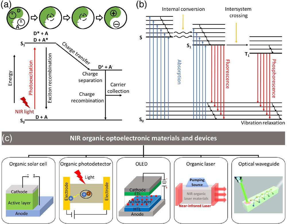
    Fig. 1. (a) Mechanism of photogenerated charge transfer. (b) Mechanisms of fluorescence and phosphorescence. (c) Main contents of this review.
    Typical donor and acceptor materials for NIR OSCs.
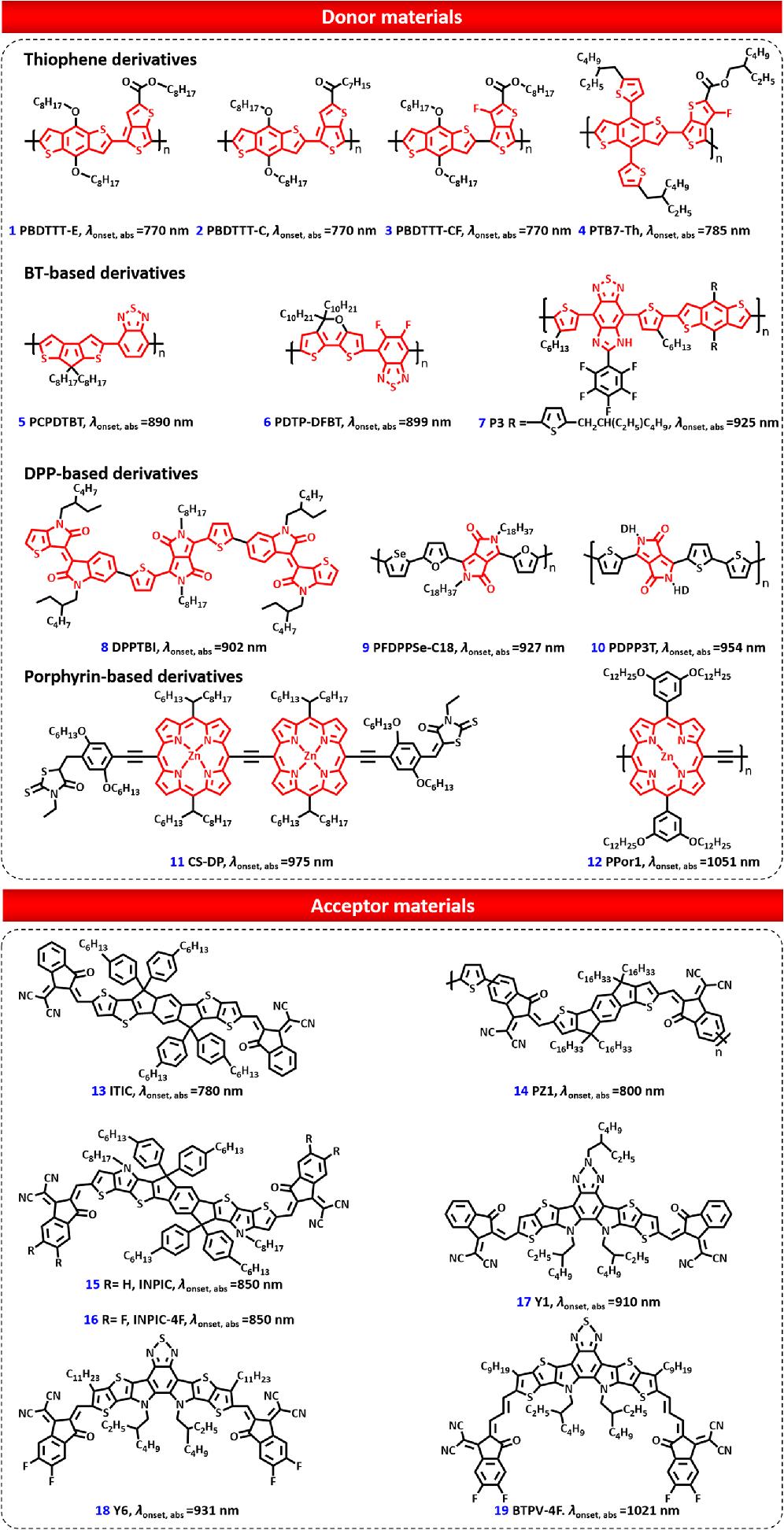
    Fig. 2. Typical donor and acceptor materials for NIR OSCs.
    (a) Device structure combining ST-OSC and 3-DM. (b) Transmission spectra of ST-OSC with different active layers. (c) Transmission spectra of different active layers added with 3-DMs. (d) Photographs of the ternary ST-OSC and glass coating. (e) Schematic diagram of the device structure of the tandem solar cell. (f) J−V curve of Tandem 1 and Tandem 2. (g) Absorption spectra of ITIC in solution (dichloromethane) and films. (h) J−V curves of PSCs with different acceptors. (i) Schematic diagrams of active layers. (j) Optical photograph of a demo [left: glass/ITO/ZnO/PBDB-T:PTAA:Y1 (6:1:9)/MoO3/Au/Ag; right: PET/Ag mesh/PEDOT:PSS PH1000/ZnO/PBDB-T:PTAA:Y1 (6:1:9)/MoO3/Au/Ag]. [(a), (b), (c), (d) Reproduced with permission,72" target="_self" style="display: inline;">72 © 2019 WILEY-VCH. (e), (f) Reproduced with permission,65" target="_self" style="display: inline;">65 © 2013 Macmillan Publishers Limited. (g), (h) Reproduced with permission,73" target="_self" style="display: inline;">73 © 2015 WILEY-VCH. (i), (j) Reproduced with permission,74" target="_self" style="display: inline;">74 © 2020 WILEY-VCH.]
    Fig. 3. (a) Device structure combining ST-OSC and 3-DM. (b) Transmission spectra of ST-OSC with different active layers. (c) Transmission spectra of different active layers added with 3-DMs. (d) Photographs of the ternary ST-OSC and glass coating. (e) Schematic diagram of the device structure of the tandem solar cell. (f) JV curve of Tandem 1 and Tandem 2. (g) Absorption spectra of ITIC in solution (dichloromethane) and films. (h) JV curves of PSCs with different acceptors. (i) Schematic diagrams of active layers. (j) Optical photograph of a demo [left: glass/ITO/ZnO/PBDB-T:PTAA:Y1 (6:1:9)/MoO3/Au/Ag; right: PET/Ag mesh/PEDOT:PSS PH1000/ZnO/PBDB-T:PTAA:Y1 (6:1:9)/MoO3/Au/Ag]. [(a), (b), (c), (d) Reproduced with permission,72 © 2019 WILEY-VCH. (e), (f) Reproduced with permission,65 © 2013 Macmillan Publishers Limited. (g), (h) Reproduced with permission,73 © 2015 WILEY-VCH. (i), (j) Reproduced with permission,74 © 2020 WILEY-VCH.]
    Representative small molecule and polymer materials for NIR OPDs.
    Fig. 4. Representative small molecule and polymer materials for NIR OPDs.
    (a) Schematic of the device structure of ultraflexible NIR OPDs. (b) Transmittance of parylene on different substances. (c) Photograph of fingerprint-conformal NIR OPDs, and the inset indicates the position of the skin-conformal NIR OPDs on the finger. (d) Device structure of the NIR OPDs. (e) Absorption spectra of PTB7-Th (red), CO1-4Cl (blue), and their BHJ blend (purple) in thin films. (f) Working principle of NIR photoplethysmography. [(a)–(c) Reproduced with permission,100" target="_self" style="display: inline;">100 © 2018 WILEY-VCH. (d)–(f) Reproduced with permission,107" target="_self" style="display: inline;">107 © 2019 WILEY-VCH.]
    Fig. 5. (a) Schematic of the device structure of ultraflexible NIR OPDs. (b) Transmittance of parylene on different substances. (c) Photograph of fingerprint-conformal NIR OPDs, and the inset indicates the position of the skin-conformal NIR OPDs on the finger. (d) Device structure of the NIR OPDs. (e) Absorption spectra of PTB7-Th (red), CO1-4Cl (blue), and their BHJ blend (purple) in thin films. (f) Working principle of NIR photoplethysmography. [(a)–(c) Reproduced with permission,100 © 2018 WILEY-VCH. (d)–(f) Reproduced with permission,107 © 2019 WILEY-VCH.]
    (a) Mechanism of emitting light of three generations of OLEDs. (b)–(d) Representative NIR materials for each of the three generations of OLEDs.
    Fig. 6. (a) Mechanism of emitting light of three generations of OLEDs. (b)–(d) Representative NIR materials for each of the three generations of OLEDs.
    (a) OLED EQE of the materials mentioned in the article. (b) Crystal structure and intermolecular interaction of TBSMCN. (c) EL spectra of devices with different structures of TBSMCN. (d) EQE of devices with different structures of TBSMCN at different current densities. [(b)–(d) Reproduced with permission,117" target="_self" style="display: inline;">117 © 2022 WILEY-VCH.]
    Fig. 7. (a) OLED EQE of the materials mentioned in the article. (b) Crystal structure and intermolecular interaction of TBSMCN. (c) EL spectra of devices with different structures of TBSMCN. (d) EQE of devices with different structures of TBSMCN at different current densities. [(b)–(d) Reproduced with permission,117 © 2022 WILEY-VCH.]
    (a) Molecular structures of LDS 798. (b) Schematic illustration of the formation of LDS 798@rho-ZMOF microcrystals via an ion exchange process. (c) Room-temperature PL spectra of an individual LDS 798@rho-ZMOF microcrystal under different pump densities at 532 nm. (d1)–(d3) The molecular structures of compounds 64, 65, and 66. (e) PL spectra of compound 64 in doped films at different pumping energies. (f) Laser emission spectra of compound 64 in doped films of different concentrations. (g1) Schematic diagram of the dye-doped film. (g2) The lasing emission spectra from the active waveguide with the FP cavity at increasing excitation levels near the threshold. (h) Molecular structure of ADH. (i) Calculated relative energies (kcal mol−1) of the TA and TB forms of NDH. (j) Laser emission spectra of ADH in PS spheres. [(b), (c) Reproduced with permission,162" target="_self" style="display: inline;">162 © 2018 American Chemical Society (ACS). (e), (f) Reproduced with permission,161" target="_self" style="display: inline;">161 © 2018 ACS. (g2) Reproduced with permission,158" target="_self" style="display: inline;">158 © 2008 American Institute of Physics. (i), (j) Reproduced with permission,159" target="_self" style="display: inline;">159 © 2020 WILEY-VCH.]
    Fig. 8. (a) Molecular structures of LDS 798. (b) Schematic illustration of the formation of LDS 798@rho-ZMOF microcrystals via an ion exchange process. (c) Room-temperature PL spectra of an individual LDS 798@rho-ZMOF microcrystal under different pump densities at 532 nm. (d1)–(d3) The molecular structures of compounds 64, 65, and 66. (e) PL spectra of compound 64 in doped films at different pumping energies. (f) Laser emission spectra of compound 64 in doped films of different concentrations. (g1) Schematic diagram of the dye-doped film. (g2) The lasing emission spectra from the active waveguide with the FP cavity at increasing excitation levels near the threshold. (h) Molecular structure of ADH. (i) Calculated relative energies (kcalmol1) of the TA and TB forms of NDH. (j) Laser emission spectra of ADH in PS spheres. [(b), (c) Reproduced with permission,162 © 2018 American Chemical Society (ACS). (e), (f) Reproduced with permission,161 © 2018 ACS. (g2) Reproduced with permission,158 © 2008 American Institute of Physics. (i), (j) Reproduced with permission,159 © 2020 WILEY-VCH.]
    (a) Molecular structures of 67, 68, 69. (b1), (b2) PL spectra of compounds 67 and 68. (c) Images of 1R, 1O, heated 1O, and the heated phase transition of 1O. (d) PL spectra of 1R. (e) Chemical structures of representative materials. (f) PL spectra of 11.5 μm long single nanowires excited by different pump energies. Inset: SEM image of organic nanowires. (g) Schematic of one nanowire on a glass substrate pumped by 532 nm laser excitation. (h) Fluorescence microscopy image of these as-prepared DMHC organic nanowire arrays. (i) PL spectra based on a single nanowire with a length of 10 μm excited at different energies at room temperature. (j) Multimode laser spectra of the selected DP-DHAQ microplate when excited by a pulsed laser (532 nm). Inset: fluorescence microscopy image of the selected microplate above the lasing threshold. [(b1), (b2) Reproduced with permission,163" target="_self" style="display: inline;">163 © 2015 WILEY-VCH. (c), (d) Reproduced with permission,164" target="_self" style="display: inline;">164 © 2016 WILEY-VCH. (f) Reproduced with permission,169" target="_self" style="display: inline;">169 © 2021 WILEY-VCH. (g)–(i) Reproduced with permission,168" target="_self" style="display: inline;">168 © 2020 Elsevier Inc. (j) Reproduced with permission,171" target="_self" style="display: inline;">171 © 2022 WILEY-VCH.]
    Fig. 9. (a) Molecular structures of 67, 68, 69. (b1), (b2) PL spectra of compounds 67 and 68. (c) Images of 1R, 1O, heated 1O, and the heated phase transition of 1O. (d) PL spectra of 1R. (e) Chemical structures of representative materials. (f) PL spectra of 11.5  μm long single nanowires excited by different pump energies. Inset: SEM image of organic nanowires. (g) Schematic of one nanowire on a glass substrate pumped by 532 nm laser excitation. (h) Fluorescence microscopy image of these as-prepared DMHC organic nanowire arrays. (i) PL spectra based on a single nanowire with a length of 10  μm excited at different energies at room temperature. (j) Multimode laser spectra of the selected DP-DHAQ microplate when excited by a pulsed laser (532 nm). Inset: fluorescence microscopy image of the selected microplate above the lasing threshold. [(b1), (b2) Reproduced with permission,163 © 2015 WILEY-VCH. (c), (d) Reproduced with permission,164 © 2016 WILEY-VCH. (f) Reproduced with permission,169 © 2021 WILEY-VCH. (g)–(i) Reproduced with permission,168 © 2020 Elsevier Inc. (j) Reproduced with permission,171 © 2022 WILEY-VCH.]
    (a) Fluorescence microscopy images of Pb-Bpeb. Inset: molecular structure of Pb-Bpeb. (b) 1D crystal by exciting the individual crystals at different positions with a laser beam (λ=405 nm). (c) Intensity ratio Itip/Ibody against the distance. (d) Molecular structure of DHNBP and the diagram of the primary branched microwire. (e) Schematic illustration of the experimental setup used for optical waveguide measurement. (f) FM images obtained from an individual TP-F4TCNQ microwire by excitation with a laser beam (λ=375 nm) at different positions with a scale bar of 50 μm. (g) Corresponding spatially resolved PL spectra in (f) with different separation distances. Inset: ratios of the intensity Itip/Ibody against the distance d. (h) Molecular structure of DCA and DPI, schematic representation of the waveguide with relative dimensions, and the procedure for manual loading with PDI crystals. [(a)–(c) Reproduced with permission,177" target="_self" style="display: inline;">177 © 2021 ACS. (e)–(g) Reproduced with permission,178" target="_self" style="display: inline;">178 © 2022 WILEY-VCH.]
    Fig. 10. (a) Fluorescence microscopy images of Pb-Bpeb. Inset: molecular structure of Pb-Bpeb. (b) 1D crystal by exciting the individual crystals at different positions with a laser beam (λ=405  nm). (c) Intensity ratio Itip/Ibody against the distance. (d) Molecular structure of DHNBP and the diagram of the primary branched microwire. (e) Schematic illustration of the experimental setup used for optical waveguide measurement. (f) FM images obtained from an individual TP-F4TCNQ microwire by excitation with a laser beam (λ=375  nm) at different positions with a scale bar of 50  μm. (g) Corresponding spatially resolved PL spectra in (f) with different separation distances. Inset: ratios of the intensity Itip/Ibody against the distance d. (h) Molecular structure of DCA and DPI, schematic representation of the waveguide with relative dimensions, and the procedure for manual loading with PDI crystals. [(a)–(c) Reproduced with permission,177 © 2021 ACS. (e)–(g) Reproduced with permission,178 © 2022 WILEY-VCH.]
    Present challenges in organic NIR optoelectronic materials.
    Fig. 11. Present challenges in organic NIR optoelectronic materials.
    DonorEgopt(eV)aHOMO/LUMO (eV)AcceptorVOC(V)bJSC(mAcm2)cFF (%)dPCE (%)eRef.
    Thiophene derivativesPBDTTT-E1.61−5.01/−3.24PC70BM0.6213.2635.1558
    PBDTTT-C1.61−5.12/−3.35PC70BM0.714.764.16.5858
    PBDTTT-CF1.61−5.22/−3.45PC70BM0.7615.266.97.7358
    PTB7-Th1.58−5.22/−3.64PC71BM0.8015.7374.39.3559
    DPP-based derivativesDPPTBI1.40−4.87/−3.47PC61BM0.692.02530.7460
    PDPP3T1.30−5.17/−3.61PC70BM0.6611.8604.6961
    PFDPPSe-C181.34−5.46/−3.81PC71BM0.641660.46.1662
    BT-based derivativesP31.34−5.72/−3.95PC71BM0.766.7638.61.9263
    PCPDTBT1.40−5.30/−3.57PC71BM0.62211473.1664
    PDTP-DFBT1.38−5.26/−3.61PC71BM0.6817.865.07.965
    Porphyrin-based derivativesCS-DP1.26−4.96/−3.74PC71BM0.78115.1469.88.2966
    PPor11.18−5.14/−3.96PC61BM0.6011.86584.1067
    Table 1. Optoelectronic and photovoltaic properties of representative NIR donor materials in OSCs.
    AcceptorEgopt (eV)aHOMO/LUMO (eV)DonorVOC (V)bJSC (mAcm2)cFF (%)dPCE (%)eRef.
    ITIC1.59−5.48/−3.83PTB7-Th0.8114.2159.16.8073
    PZ11.55−5.74/−3.86PBDB-T0.8316.0568.999.1987
    INPIC1.46−5.36/−3.82PBDB-T0.968.5552.54.3188
    INPIC-4F1.39−5.42/−3.94PBDB-T0.8521.6171.513.1388
    Y11.44−5.45/−3.95PBDB-T0.8722.4469.113.4274
    Y61.33−5.65/−4.10PM60.8325.374.815.789
    BTPV-4F1.21−5.39/−4.08PTB7-Th0.6528.365.912.190
    Table 2. Optoelectronic and photovoltaic properties of representative NIR acceptor materials in OSCs.
    MaterialEgopt (eV)aSpectral region (nm)λabs,max(nm)Jd(A/cm2)bλdet (nm) / Vbias (V)cD*(Jones)dR(A/W)eRef.
    PolymerPTT1.30400 to 970750NA850/−5NA0.2698
    PIPCP1.50300 to 1000800NA800/−21.34×10110.14499, 100
    PDDTT0.80300 to 14508601010800/−0.12.3×1013NA101
    PPhTQ0.80700 to 15001143400102
    PBBTPD1.44350 to 250012001×1091500/−0.52.2×10111.4×107103
    Small moleculeF16CuPc1.4–1.5400 to 80078513.6104
    DHTBTEZP1.30380 to 9608013.44×1010800/04.56×1012NA105
    TET-CN1.40500 to 9008309×104106
    CO1-4Cl1.19400 to 1100920NA920/−210120.53107
    NTQ1.11320 to 10709541.5×105980/−23.72×10120.24108
    Compound 300.80400 to 150010241.1×1051390/01.7×1010NA109
    Compound 310.85400 to 14609961.4×1081140/05.3×1010NA109
    Table 3. Optoelectronic properties for polymer and small molecule absorption materials and devices incorporating them.
    CompoundλPL,max (nm)a (solution/film)λEL,max (nm)bΦPL (%)cMax EQE (%)dRef.
    Compound 421285/NA12200.5NA121
    Compound 401080/106010805.80.73121
    Compound 411040/104010506.30.33121
    Compound 391055/105010507.40.16121
    1a700/70470636.90.89122
    1b780/7617498.20.29122
    2a787/8038020.260.43122
    2b857/8838646.390.20122
    P240NA/890895NA0.091123
    P3NA/927939NA0.006123
    P4NA/1000990NA0.018123
    Table 4. Optoelectronic properties for representative fluorescent materials and corresponding devices.
    CompoundλPL,max(nm)aλEL,max(nm)bΦPL(%)cMax EQE (%)dRef.
    ErQ15221533NANA127, 128
    NIR 1720720NA0.25129
    PtTPTBP77077051.08.0130
    PtNTBP84284822.02.8130
    cis-PtN2TBP83084617.01.5130
    Compound 487407408124131
    DR96599513.32.42132
    D(8)-DR96599519.54.08132
    per-DR96599522.84.31132
    MeDR92093016.03.66132
    D-MeDR92093026.06.25132
    5tBuDR85588218.13.78132
    PhDR970100213.22.71132
    Table 5. Optoelectronic properties for representative phosphorescent materials and corresponding devices.
    CompoundΔEST (eV)aλPL,max (nm)bλEL,max (nm)cΦPL (%)dMax EQE (%)eRef.
    TPA-DCPP0.13708668149.8139
    TPA-QCN0.23733728213.9140
    APDC-DTPA0.14687, 756698, 77763 (@687 nm), 13 (@756 nm)10.19 (@693 nm), 2.19 (@777 nm)141
    PXZ-TRZNANA9700.30.1142
    TPA-PZTCN0.14729734, 90140.813.4 (@734 nm), 1.1 (@901 nm)143
    TBSMCN0.1782080410.72.17117
    Table 6. Optoelectronic properties for TADF materials and corresponding devices.
    MaterialλPL,max (nm)λlaser,center (nm)Threshold (μJcm2)Ref.
    Dye-doped NIR laserLSD950/FPI960970220158
    ADH/PS75086027.4159
    Compound 63/CBP706 to 782740 to 7995 to 37160
    Compound 64/CBD751 to 801801 to 8607.5 to 91.4161
    LDS 798/rho ZMOF75079017.2162
    NIR laser in crystal stateDMHAC7107149.2  kWcm2163
    Compound 68716716100  kWcm2163
    DFHP70271420.8  kWcm2164
    DPHP5967000.61 (TM mode), 0.75 (TE mode)165
    DMHP6757201.4166
    DEPHP700 (α-phase), 728 (β-phase)7301.86167
    DMHC7007759.9168
    DDMP77885413.2169
    TPE-SP6607203.68170
    DP-DHAQ66072526.9171
    H2TPyP655 (0-0), 716 (0-1)7320.119172
    Table 7. Properties of NIR OSSLs.
    Zong-Lu Che, Chang-Cun Yan, Xue-Dong Wang, Liang-Sheng Liao. Organic near-infrared optoelectronic materials and devices: an overview[J]. Advanced Photonics, 2024, 6(1): 014001
    Download Citation