• Chinese Physics B
  • Vol. 29, Issue 8, (2020)
Ateyyah M Al-Baradi1、†, Fatimah A Altowairqi1, A A Atta1、2, Ali Badawi1, Saud A Algarni1, Abdulraheem S A Almalki3, A M Hassanien4, A Alodhayb5, A M Kamal6, and M M El-Nahass2
Author Affiliations
  • 1Department of Physics, Faculty of Science, Taif University, Taif 2974, Saudi Arabia
  • 2Department of Physics, Faculty of Education, Ain Shams University, Roxy 11757, Cairo, Egypt
  • 3Department of Chemistry, Faculty of Science, Taif University, Taif, Saudi Arabia
  • 4Department of Physics, College of Science and Humanities – Al Quwaiiyah, Shaqra University, Saudi Arabia
  • 5Research Chair for Tribology, Surface, and Interface Sciences, Department of Physics and Astronomy, College of Science, King Saud University, Riyadh 1141, Saudi Arabia
  • 6Department of Physics and Astronomy, College of Science, King Saud University, Riyadh 11451, Saudi Arabia
  • show less
    DOI: 10.1088/1674-1056/ab90e6 Cite this Article
    Ateyyah M Al-Baradi, Fatimah A Altowairqi, A A Atta, Ali Badawi, Saud A Algarni, Abdulraheem S A Almalki, A M Hassanien, A Alodhayb, A M Kamal, M M El-Nahass. Structural and optical characteristic features of RF sputtered CdS/ZnO thin films[J]. Chinese Physics B, 2020, 29(8): Copy Citation Text show less
    FTIR spectra of as-deposited and thermally annealed CdS/ZnO thin films.
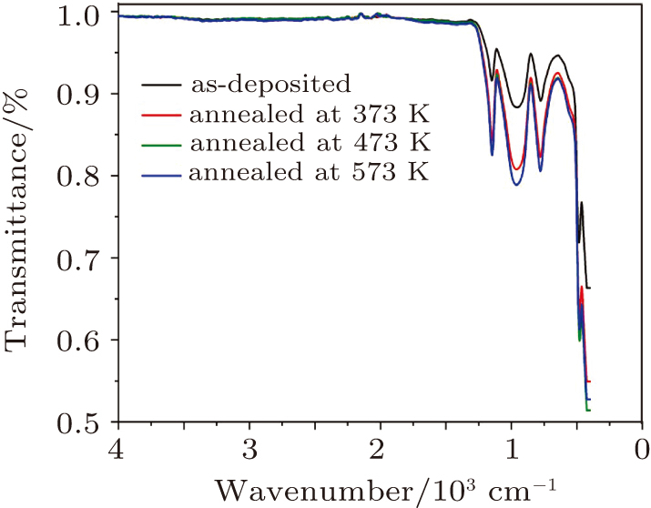
    Fig. 1. FTIR spectra of as-deposited and thermally annealed CdS/ZnO thin films.
    Observed XRD patterns of as-deposited and thermally annealed CdS/ZnO thin films.
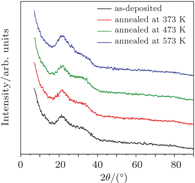
    Fig. 2. Observed XRD patterns of as-deposited and thermally annealed CdS/ZnO thin films.
    FESEM micrographs of as-deposited and thermally annealed CdS/ZnO thin films as a function of temperatures: (a) as-deposited film, (b) annealed film at 373 K, (c) annealed film at 473 K, and (d) annealed film at 573 K.
    Fig. 3. FESEM micrographs of as-deposited and thermally annealed CdS/ZnO thin films as a function of temperatures: (a) as-deposited film, (b) annealed film at 373 K, (c) annealed film at 473 K, and (d) annealed film at 573 K.
    The absorbance spectra of as-deposited and thermally annealed CdS/ZnO thin films.
    Fig. 4. The absorbance spectra of as-deposited and thermally annealed CdS/ZnO thin films.
    Transmittance and reflectance spectra of asdeposited and thermally annealed CdS/ZnO thin films.
    Fig. 5. Transmittance and reflectance spectra of asdeposited and thermally annealed CdS/ZnO thin films.
    Spectral dependence of absorption coefficient of as-deposited and thermally annealed CdS/ZnO thin films with inset showing energy dependence of ln(α) for as-deposited and thermally annealed CdS/ZnO.
    Fig. 6. Spectral dependence of absorption coefficient of as-deposited and thermally annealed CdS/ZnO thin films with inset showing energy dependence of ln(α) for as-deposited and thermally annealed CdS/ZnO.
    Plots of (αhν)1/2versus hν for as-deposited and thermally annealed CdS/ZnO thin films.
    Fig. 7. Plots of (αhν)1/2versus hν for as-deposited and thermally annealed CdS/ZnO thin films.
    Room-temperature PL spectra of as-deposited and thermally annealed CdS/ZnO thin films excited at 300 nm.
    Fig. 8. Room-temperature PL spectra of as-deposited and thermally annealed CdS/ZnO thin films excited at 300 nm.
    De-convoluted analysis of annealed CdS/ZnO thin film at 573 K.
    Fig. 9. De-convoluted analysis of annealed CdS/ZnO thin film at 573 K.
    Spectral dependence of mean real part of refractive index, n, of as-deposited and thermally annealed CdS/ZnO thin films.
    Fig. 10. Spectral dependence of mean real part of refractive index, n, of as-deposited and thermally annealed CdS/ZnO thin films.
    Plots of (n2 − 1)−1versus (hν)2 for as-deposited and thermally annealed of CdS/ZnO thin films.
    Fig. 11. Plots of (n2 − 1)−1versus ()2 for as-deposited and thermally annealed of CdS/ZnO thin films.
    Plots of n2versusλ2 for as-deposited and thermally annealed of CdS/ZnO thin films.
    Fig. 12. Plots of n2versusλ2 for as-deposited and thermally annealed of CdS/ZnO thin films.
    Spectral behaviors of third-order nonlinear susceptibility, χ(3) for as-deposited and thermally annealed of CdS/ZnO thin films.
    Fig. 13. Spectral behaviors of third-order nonlinear susceptibility, χ(3) for as-deposited and thermally annealed of CdS/ZnO thin films.
    Spectral behaviors of nonlinear refractive index n2 for as-deposited and thermally annealed of CdS/ZnO thin films.
    Fig. 14. Spectral behaviors of nonlinear refractive index n2 for as-deposited and thermally annealed of CdS/ZnO thin films.
    Material of the targetCdS/ZnO (2:3 mol%) Applied Science Crop.
    Sputtering gasAr (99.99%)
    Substratequartz at room temperature (2 cm × 2 cm)
    Substrate temperature/K300
    Target substrate distance and angle10 cm with an angle 65°
    RF Sputtering power/W150
    Pure Ar flow rate (standard cubic centimeter per minute)30 cm3/min
    Sputtering pressure (Pchamber)/mbar2.6 × 10−2
    Substrate rotation/rpm10
    Target size3-inch diameter × 5-mm thickness
    Deposition time/h6
    Thin film thickness/nm515
    Deposition rate/(nm/min)1.43
    Annealing temperature (air and atmospheric pressure)/K373, 473, 573
    Table 1. Experimental parameters of sputtering-deposited CdS/ZnO thin films.
    Optical parametersEgind./eVEu/meVEo/eVEd/eVεεL(N/m*)/1047 g−1⋅ cm−3
    As-deposited2.601924.09520.1775.9266.082.326
    373 K2.601833.95118.215.6085.792.43
    473 K2.631503.76715.8955.21945.191.753
    573 K2.501794.43415.2374.4364.380.956
    Table 2. Optical parameters of transparent CdS/ZnO thin films.
    Ateyyah M Al-Baradi, Fatimah A Altowairqi, A A Atta, Ali Badawi, Saud A Algarni, Abdulraheem S A Almalki, A M Hassanien, A Alodhayb, A M Kamal, M M El-Nahass. Structural and optical characteristic features of RF sputtered CdS/ZnO thin films[J]. Chinese Physics B, 2020, 29(8):
    Download Citation