
Wenfu Yu, Xuyi Zhao, Shixian Han, Antian Du, Ruotao Liu, Chunfang Cao, Jinyi Yan, Jin Yang, Hua Huang, Hailong Wang, Qian Gong, "InAs/GaAs quantum dot laterally coupled distributed feedback lasers at 1.3 μm," Chin. Opt. Lett. 21, 011402 (2023)
- Chinese Optics Letters
- Vol. 21, Issue 1, 011402 (2023)
Abstract
1. Introduction
High performance, reliable, and low cost semiconductor lasers are crucial for applications in the field of optical communication[1]. While single-channel optical interconnects can operate with electrically pumped Fabry–Perot lasers, distributed-feedback (DFB) lasers, which provide single-longitudinal-mode emission with a narrow spectrum line width, are indispensable for wavelength division multiplexing systems[2]. A number of advantages of the GaAs-based InAs quantum dot (QD) laser diodes operating in the 1310 nm wavelength region have been found over the commercial InP-based III–V quantum well (QW) lasers, such as low threshold current density, high quantum efficiency (QE), and high temperature stability[3–6]. Moreover, a very important advantage of QD lasers is that the QDs active region has been proved to be much less sensitive to crystal defects than in the conventional QW structures due to effective three-dimensional carrier localization[7]. Thus, InAs QDs are desirable to be utilized for the active region of silicon-based lasers[8,9]. The InAs/InGaAs QDs DFB laser becomes very important in the development of silicon-based photonics. Although the electrically pumped DFB laser using InAs/GaAs QD gain material epitaxially grown on silicon was reported by Wang et al.[10], there is still very little research effort on InAs QD DFB lasers[11,12].
In this work, we report the fabrication and characterization of 1.31 µm GaAs-based QD laterally coupled DFB (LC-DFB) lasers by employing the first-order Cr gratings. Excellent single-longitudinal-mode characteristics with a high side mode suppression ratio (SMSR) above 52 dB have been achieved. With an injection current of 300 mA, the LC-DFB laser emits up to 5 mW per facet.
2. Experimental Procedure
The laser structure was grown on 4 in. n-type GaAs (001) substrates by a solid source molecular beam epitaxy system equipped with an As cracker. The grown structure was started with a 500 nm GaAs buffer layer deposited at 720°C after native oxide desorption. Then, a 1.5 µm n-doped
Sign up for Chinese Optics Letters TOC. Get the latest issue of Chinese Optics Letters delivered right to you!Sign up now
Narrow ridge waveguide DFB lasers were fabricated with ridge width of 3 µm. The ridge structures were defined by optical lithography followed by chlorine-based inductively coupled plasma reactive ion etching. The etching was stopped when the depth reaches the active region. Then, Cr gratings were fabricated alongside the ridge waveguide by electron beam lithography and lift-off process. A 200-nm-thick
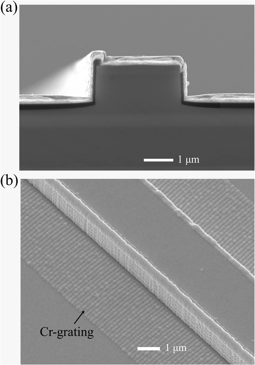
![]()
Figure 1.SEM image of the LC-DFB laser. (a) Cross-section view. (b) Top view.
3. Result and Discussion
Laser diodes with cavity length of 4 mm were cleaved and mounted epi-side up on copper heat sinks by In soldering. Both facets were left uncoated. Narrow ridge lasers were measured in continuous-wave (CW) mode. The output power was measured by an integrating sphere InGaAs photodiode power sensor S145C from Thorlabs. For CW mode, a current and temperature controller ITC4020 from Thorlabs was used for current injection and heat sink temperature control. The device operating temperature was monitored by a resistance temperature detector PT100 mounted alongside the copper heatsink. An IS-50R Fourier transform infrared spectrometer and an OSA20 spectrum analyzer were used to record the lasing spectra.
The CW mode current-voltage-power (I-V-P) characteristics of an LC-DFB laser with 4-mm-long cavity and 3.0-µm-wide ridge are shown in Fig. 2(a). The laser has a threshold of 207 mA at 20°C, corresponding to a threshold current density of
![]()
Figure 2.(a) I-V-P characteristic of the LC-DFB laser in CW mode at 20°C. (b) The relationship between peak wavelength and current from 220 mA to 280 mA of the LC-DFB laser.
The laser diode was systematically characterized in the temperature range of 10°C–30°C. Characteristic temperature
![]()
Figure 3.(a) Characteristic temperature T0 calculated under CW mode from 10°C to 30°C. (b) Variation of external efficiency calculated under CW mode from 10°C to 30°C.
Under CW operation, the lasing wavelength can be tuned by varying the injection current and operating temperature. Lasing spectra the LC-DFB laser collected at 20°C are shown in Fig. 4(a), with injection currents varying from 230 mA to 350 mA in steps of 10 mA. In this current range, it is found that the LC-DFB laser is running as mode-hop free with very high SMSR values. Figure 4(b) shows the dependence of operating wavelength and SMSR on the injection current at different temperatures in the range of 10°C–30°C. A wavelength window of 1311.5–1314.5 nm can be covered by the LC-DFB laser operating in single mode. The tuning rates of the lasing wavelength with current and temperature are 4.15 pm/mA and 0.12 nm/K, respectively. As shown in Fig. 4(b), for all the operating parameters (i.e., temperatures and injection currents), the SMSR over 40 dB were measured exclusively. The maximum SMSR has been obtained over 50 dB, indicating that the device has excellent single-mode operation performance[21]. Figure 5 shows a lasing spectrum of the LC-DFB laser, where the maximum SMSR of 52 dB has been achieved at 20°C with an injection current of 290 mA and a lasing wavelength of 1313.27 nm. This maximum SMSR value is better than that of most commercially available DFB lasers in this wavelength region[22]. The outstanding SMSR performance is attributed to the good match of mode wavelength selected by the Cr gratings and the peak of the gain profile.
![]()
Figure 4.(a) Spectra of the LC-DFB laser with injection current from 230 mA to 350 mA with a step of 10 mA at 20°C. (b) Variation of emission wavelength and SMSR versus current at different temperatures.
![]()
Figure 5.Lasing spectrum of the LC-DFB laser with high SMSR ratio.
InAs/GaAs QD gain material has a unique feature, i.e., its gain profile is much broader than that of the conventional QW structure. Thus, it is possible to fabricate a single chip that integrates several laser diodes covering a broad wavelength range, e.g., the wavelength span of the O-band four-wavelength coarse wavelength division multiplexing (CWDM) application (i.e., 60 nm). We tentatively explored the feasibility mentioned above by fabricating three LC-DFB lasers on a single chip. The operating wavelengths in the multi-laser chip were slightly different from the lasers discussed before, since a different epi-wafer was used for this purpose with gain peak located at shorter wavelength. As shown in Fig. 6, three operating wavelengths are achieved in a single chip integrating three LC-DFB lasers, while the wavelengths were determined by different periods of the gratings. The laser spectra were measured using a Fourier transform infrared spectrometer, in which a liquid-nitrogen cooled InSb detector and a
![]()
Figure 6.Spectra of the LC-DFB laser arrays in CW mode at 20°C.
4. Conclusion
In conclusion, we have demonstrated high performance GaAs-based InAs QDs LC-DFB lasers employing Cr metal gratings along the ridge side. Single-mode operation was achieved in CW mode at room temperature, with SMSR in the range of 40–52 dB and output power of 5 mW. Wavelength tuning properties were characterized, and the tuning rates of 4.15 pm/mA and 0.12 nm/K were obtained, respectively. Moreover, a single chip integrating three LC-DFB lasers was tentatively explored. It is found that each LC-DFB laser on the chip can operate in single mode at room temperature. The chip was able to cover the wavelength span of 35.6 nm, showing significant potential in the CWDM applications.
References
[1] B. Dagens, J. Renaudier, R. Brenot, A. Accard, F. van Dijk, D. Make, O. Le Gouezigou, J.-G. Provost, F. Poingt, J. Landreau, O. Drisse, E. Derouin, B. Rousseau, F. Pommereau, G.-H. Duan. Recent advances on InAs/InP quantum dash based semiconductor lasers and optical amplifiers operating at 1.55 µm. IEEE J. Sel. Top. Quantum Electron., 13, 111(2007).
[2] C. P. Joseph. Fiber Optic Communications(2005).
[3] Q. Li, X. Wang, Z. Zhang, H. Chen, Y. Huang, C. Hou, J. Wang, R. Zhang, J. Ning, J. Min, C. Zheng. Development of modulation p-doped 1310 nm InAs/GaAs quantum dot laser materials and ultrashort cavity Fabry-Perot and distributed-feedback laser diodes. ACS Photonics, 5, 1084(2018).
[4] G. Liu, A. Stintz, H. Li, K. Malloy, L. Lester. Extremely low room-temperature threshold current density diode lasers using InAs dots in In0.15Ga0.85As quantum well. Electron. Lett., 35, 1163(1999).
[5] M. Asada, Y. Miyamoto, Y. Suematsu. Gain and the threshold of three-dimensional quantum-box lasers. IEEE J. Quantum Electron., 22, 1915(1986).
[6] O. B. Shchekin, D. G. Deppe. 1.3 µm InAs quantum dot laser with To = 161 K from 0 to 80°C. Appl. Phys. Lett., 80, 3277(2002).
[7] Z. T. Mi, J. Yang, P. Bhattacharya, G. X. Qin, Z. Q. Ma. High-performance quantum dot lasers and integrated optoelectronics on Si. Proc. IEEE, 97, 1239(2009).
[8] K. Nishi, K. Takemasa, M. Sugawara, Y. Arakawa. Development of quantum dot lasers for data-com and silicon photonics applications. IEEE J. Sel. Top. Quantum Electron., 23, 1901007(2017).
[9] A. Y. Liu, C. Zhang, J. Norman, A. Snyder, D. Lubyshev, J. M. Fastenau, A. W. K. Liu, A. C. Gossard, J. E. Bowers. High performance continuous wave 1.3 µm quantum dot lasers on silicon. Appl. Phys. Lett., 104, 041104(2014).
[10] Y. Wang, S. Chen, Y. Yu, L. Zhou, L. Liu, C. Yang, M. Liao, M. Tang, Z. Liu, J. Wu, W. Li, I. Ross, A. J. Seeds, H. Liu, S. Yu. Monolithic quantum-dot distributed feedback laser array on silicon. Optica, 5, 528(2018).
[11] Y. Qiu, P. Gogna. Laterally coupled InAs quantum dot distributed feedback lasers at 1.3 µm. IEEE-NANO(2003).
[12] S. R. Jain, M. N. Sysak, G. Kurczveil, J. E. Bowers. Integrated hybrid silicon DFB laser-EAM array using quantum well intermixing. Opt. Express, 19, 13692(2011).
[13] M. J. Wallace, Q. Lu, W.-H. Guo, J. F. Donegan. Design optimization for semiconductor lasers with high-order surface gratings having multiple periods. J. Light. Technol., 36, 5121(2018).
[14] C.-A. Yang, S.-W. Xie, Y. Zhang, J.-M. Shang, S.-S. Huang, Y. Yuan, F.-H. Shao, Y. Zhang, Y.-Q. Xu, Z.-C. Niu. High-power, high-spectral-purity GaSb-based laterally coupled distributed feedback lasers with metal gratings emitting at 2 µm. Appl. Phys. Lett., 114, 021102(2019).
[15] H. Kogelnik, C. V. Shank. Coupled-wave theory of distributed feedback lasers. J. Appl. Phys., 43, 2327(1972).
[16] W. Streifer, D. Scifres, R. Burnham. Coupling coefficients for distributed feedback single- and double-heterostructure diode lasers. IEEE J. Quantum Elect., 11, 867(1975).
[17] K. Papatryfonos, D. Saladukha, K. Merghem, S. Joshi, F. Lelarge, S. Bouchoule, D. Kazazis, S. Guilet, L. Le Gratiet, T. J. Ochalski, G. Huyet, A. Martinez, A. Ramdane. Laterally coupled distributed feedback lasers emitting at 2 µm with quantum dash active region and high-duty-cycle etched semiconductor gratings. J. Appl. Phys., 121, 053101(2017).
[18] B. Dong, J. Duan, H. Huang, J. C. Norman, K. Nishi, K. Takemasa, M. Sugawara, J. E. Bowers, F. Grillot. Dynamic performance and reflection sensitivity of quantum dot distributed feedback lasers with large optical mismatch. Photonics. Res., 9, 1550(2021).
[19] L. Jiang, L. V. Asryan. Excited-state-mediated capture of carriers into the ground state and the saturation of optical power in quantum-dot lasers. IEEE Photon. Technol. Lett., 18, 2611(2006).
[20] L. V. Asryan, R. A. Suris. Spatial hole burning and multimode generation threshold in quantum-dot lasers. Appl. Phys. Lett., 74, 1215(1999).
[21] J. Wang, C. Z. Sun, B. Xiong, Y. Luo, Z. B. Hao, Y. J. Han, L. Wang, H. T. Li, J. D. Yu. 1.3 µm laterally coupled distributed feedback laser with high side mode suppression ratio and bandwidth. Asia Communications and Photonics Conference (ACPC), T3D.3(2019).
[22] R. Millett, K. Dridi, A. Benhsaien, H. Schriemer, K. Hinzer, T. Hall. Fabrication-tolerant 1310 nm laterally coupled distributed feedback lasers with high side mode suppression ratios. Photonics Nanostruct., 9, 111(2011).


Set citation alerts for the article
Please enter your email address

© Copyright 2018-2021 | Chinese Laser Press. All Rights Reserved 沪ICP备15018463号-20