
Yuanhe Wang, Xinyi Li, Shihao Liu, Letian Zhang, Wenfa Xie, "Flexible top-illuminated organic photodetector using an ultrathin-metal-based transparent electrode," Photonics Res. 11, 2100 (2023)
- Photonics Research
- Vol. 11, Issue 12, 2100 (2023)
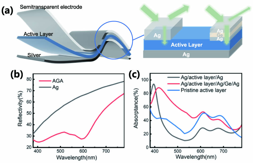
Fig. 1. (a) Structure diagram of flexible OPDs with a reflective Ag electrode and an Ag or AGA semitransparent electrode. (b) Reflectivity characteristics of the Ag film and the AGA film. (c) Absorptance spectra of the photoactive layers consisting of CuPc:C 60

Fig. 2. (a) EQE characteristics of devices Ag and AGA with a device structure: Ag ( 100 nm ) /MoO 3 ( 5 nm ) /CuPc ( 50 nm ) /CuPc : C 60 ( 50 % , 20 nm ) /C 60 C 60 C 60 C 60
Fig. 3. AFM images and schematic diagram of film growth modes of (a) 10 nm Ag (10 nm) and (b) 10 nm AGA consisting of 1 nm Ag/1 nm Ge/8 nm Ag. SEM images of (c) 10 nm Ag and (d) 10 nm AGA consisting of 1 nm Ag/1 nm Ge/8 nm Ag. (e) Transmittance and absorptance spectra of the AGA films. The red, blue, and green lines, respectively, correspond to AGA films with thicknesses of 10 nm, 15 nm, and 25 nm, respectively. The 10 nm film consists of 1 nm Ag/1 nm Ge/8 nm Ag, the 15 nm film consists of 4 nm Ag/1 nm Ge/10 nm Ag, and the 25 nm film consists of 15 nm Ag/5 nm Ge/5 nm Ag. (f) EQE characteristics of devices with the AGA films with thicknesses of 10 nm, 15 nm, and 25 nm. Its device structure is PET/Ag ( 100 nm ) /MoO 3 ( 20 nm ) /CuPc : C 60 ( 50 nm ) /C 60 ( 20 nm ) /BCP
Fig. 4. (a) EQE variation of the flexible OPDs after bending. The flexible device ITO has the same structure as the flexible device AGA, except for the ITO anode and the 100 nm Ag cathode. The insets show the device level diagram. (b) Current density-voltage characteristics of flexible device ITO and flexible device AGA. Imaging of (c) the letter “L” and (d) symbol representing a “transverse line” using 2 × 2 2 × 2
Fig. 5. (a) Simulated electric field intensity | E |


Set citation alerts for the article
Please enter your email address

© Copyright 2018-2021 | Chinese Laser Press. All Rights Reserved 沪ICP备15018463号-20