
Aba Tudahong, Yu Qu, Jun-Ran Bai, Zhong-Yue Zhang. Studies of circular dichroism of planar composite metal nanostructure arrays [J]. Acta Physica Sinica, 2020, 69(10): 107802-1
- Acta Physica Sinica
- Vol. 69, Issue 10, 107802-1 (2020)
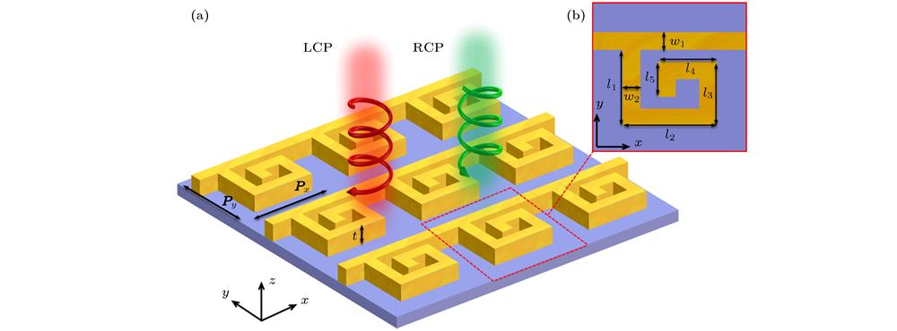
Fig. 1. Schematic of the proposed PCMN arrays: (a) Three dimensional schematic of PCMN; (b) unit schematic of PCMN in x y plane
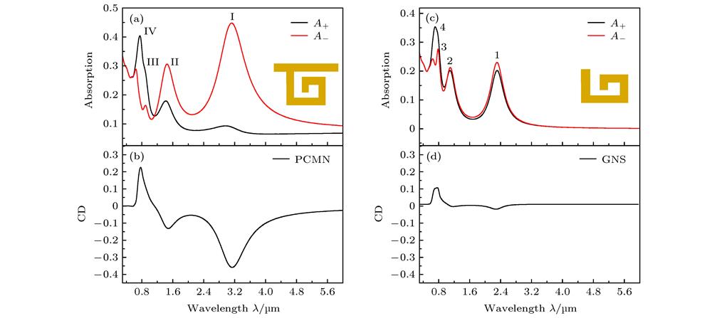
Fig. 2. Absorption and CD spectra of PCMN and GNS arrays: (a), (c) Simulated A –, A + spectra; (b), (d) CD spectra of PCMN and GNS arrays. The insert figures indicate the structure schematic of PCMN and GNS in x-y plane, respectively.
Fig. 3. Surface charge density distribution of proposed PCMN and GNS at the resonant wavelength with different circularly polarized illuminations: (a), (b), (c), (d), (i), (j), (k) and (l) for LCP light; (e), (f), (g), (h), (m), (n), (o) and (p) for RCP light.
Fig. 4. CD spectra of PCMN arrays with different parameter; CD spectraof PCMN arrays with (a) different l 1 (b) different l 2, (c) different l 3, (d) different l 4, (e) different l 5nanorod and (f) different w 1of the infinite long nanowire.
Fig. 5. Absorption and CD spectra of the separated PCMN arrays: (a) Absorption spectrum; (b) CD spectrum; The insert figures indicate the charge distribution at resonance wavelength (crimson and blue), and structure schematic (yellow) of separated PCMN in xy plane.

Set citation alerts for the article
Please enter your email address
© Copyright 2018-2021 | Chinese Laser Press. All Rights Reserved 沪ICP备15018463号-20