
Yulian He, Yuansheng Wang, Qinghui Yang, Huaiwu Zhang, Qiye Wen, "Enhanced performance of a fast GaAs-based terahertz modulator via surface passivation," Photonics Res. 9, 2230 (2021)
- Photonics Research
- Vol. 9, Issue 11, 2230 (2021)
Abstract
1. INTRODUCTION
Recently, a growing research emphasis has been placed on terahertz (THz) radiation in view of its unique properties and potential applications in spectroscopy, noninvasive testing, and high-speed communications [1–3]. Being an imperative component in actual THz systems, considerable progress has been achieved in active modulators. These modulators are capable of complete adaptive manipulation of THz waves, primarily via electric, optical, or thermal stimuli. Among these, quasi-optical manipulation that allows fast transfer of information from the optical to THz regime is of particular interest [4]. A simple, but remarkable, opto-THz modulator is based on semiconductors, such as silicon (Si), germanium (Ge), or gallium arsenide (GaAs). When the semiconductor is irradiated by a laser with the photo energy larger than its bandgap, free carriers will be generated. These generated carriers form a temporary thin conductive layer at the surface. THz waves collimated onto this region are thus attenuated due to the increased reflection and absorption [5]. This kind of device realized by varying photo-carrier populations predicts a broadband and cost-effective modulation method. Although such Si-based THz modulators are well established and significant advancement has been realized by cooperating with various heterogeneous films [6–9] and nanostructuring/microstructuring [10,11], they are mainly concentrated on photomodulation efficiency. Merely investigations on the response speed were reported. Because the carrier lifetime of Si is relatively long, typically
An alternative highly investigated semiconductor for THz modulation is GaAs. GaAs has a direct bandgap of 1.44 eV, higher electron mobility than both Si and Ge, and a rather shorter carrier lifetime, on the order of picoseconds [14]. This makes GaAs an excellent candidate to realize fast THz modulation. However, there exists a trade-off between the modulation depth (MD) and speed because the MD depends on the accumulation of carriers, where a longer
As a proof of concept, here we designed and fabricated such a performance-enhanced modulator by passivating a GaAs surface with
Sign up for Photonics Research TOC. Get the latest issue of Photonics Research delivered right to you!Sign up now
2. MATERIAL PREPARATION AND CHARACTERIZATION
The investigations were performed on the semi-insulating n-GaAs(100) wafers, with a thickness of 625 μm and dark resistivity
The optical absorption was measured by an ultraviolet/visible/infrared (UV/VIS/IR) spectroscopy (PerkinElmer Lambda 750), and the PL intensity of GaAs samples under investigation was measured by a steady-state and transient fluorescence spectrometer (Edinburgh Instruments, FLS980). By means of a homemade optically pumped terahertz-probe (OPTP) spectroscopy system, the carrier lifetime of GaAs samples was determined. The THz time-domain signals transmitted through both GaAs samples were also detected by this OPTP system. For the dynamic modulation of a continuous THz wave (
3. RESULTS AND DISCUSSION
As a measure of passivation efficiency, the PL properties in both GaAs wafers without and with surface treatment were investigated and considerably improved in the surface-passivated one. As shown in Fig. 1(a), the greatest increase of the PL intensity of S-passivated GaAs relative to bare GaAs achieves a 5.8-fold increase, which stems from the effective removal of oxides from the GaAs surface during the acid treatment and the following formation of sulfides by sulfur passivation. These courses lower the surface states and result in an attendant reduction of the surface recombination velocity [23], which indicates that a longer lifetime of surface carriers will be induced.
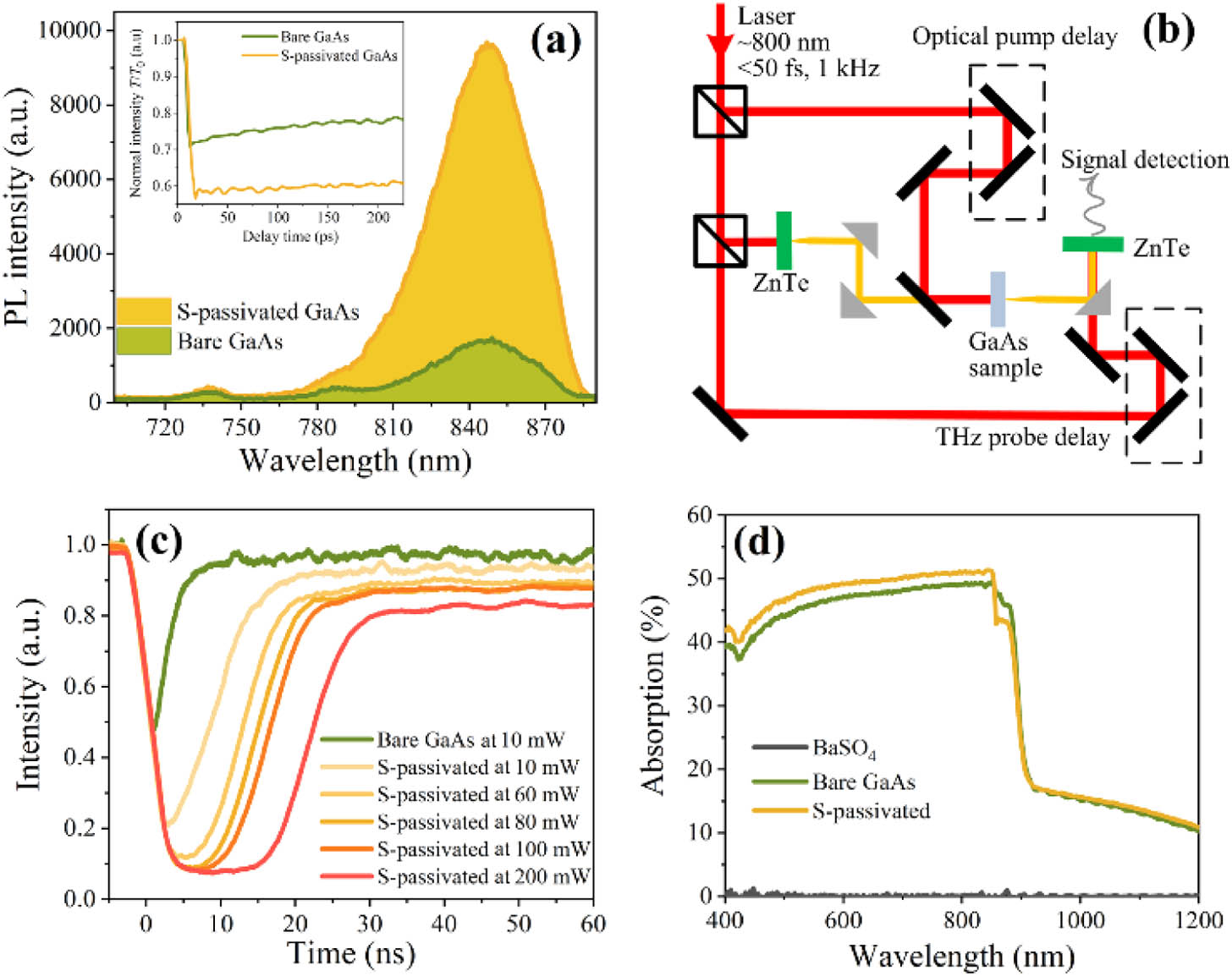
Figure 1.Characterization of GaAs wafers before and after surface passivation. (a) PL spectra (inset: time-resolved THz transmission for the S-passivated GaAs and the reference bare GaAs measured at a low fluence of 3 mW); (b) schematic of the home-made OPTP setup; (c) response waveform of the bare and S-passivated GaAs based modulators to one pulse of the laser under different power levels; and (d) measured UV/VIS/IR absorption spectra.
For the verification of the relation between PL intensity and carrier lifetime, an all-optical alternative technique (OPTP), was adopted, which is also referred to as time-resolved THz spectroscopy. This OPTP system has been demonstrated to be able to characterize optical and electrical properties of semiconductors that circumvents the need for PL and electrical contacts [24,25]. By means of this pump-and-probe scheme, an ultrashort optical pump arrives at the surface of the sample, creating a photo-carrier population that is probed by a THz pulse. By monitoring the transmission at a fixed probe position, and time-resolving the pump, the carrier lifetime can be estimated [26]. We homemade such an OPTP spectroscopy system and the setup is shown in Fig. 1(b). A femtosecond pulse laser centered at 800 nm with duration of
This type of subnanosecond carrier lifetime indicates a fast response of THz modulation. With a 340 GHz carrier, the dynamic response waveforms, through the bare and S-passivated GaAs-based modulators, to one of the pulses of the pumping laser were detected. As exhibited in Fig. 1(c), the intensities via both bare and S-passivated GaAs samples decline quickly at an almost identical speed. Then a slower recovery process is observed in the S-passivated one because the photo-generated electron-hole pairs usually can be generated in a very short time upon photodoping. Its recovery, however, is dependent on the recombination time, owing to the longer one that is positively correlated with the carrier lifetime, hence resulting in a longer recovery time after passivation. Remember the definition of response time in Ref. [5]: the time taken to modulate THz beam from 90% to 10% intensity as transfer time and that taken to return from 10% to 90% as recovery time. The response time for bare and S-passivated GaAs under 10 mW excitation was estimated to be 6.575 ns and 12.5125 ns, respectively. Hence, response rates of 154 MHz and 80 MHz can be calculated, respectively. Despite this, the speed was approximately halved in the S-passivated GaAs-based modulator due to the lengthened carrier lifetime by surface-passivating; as high as 80 MHz speed is still rather tantalizing with regard to the
We also measured the UV/VIS/IR absorption spectra of GaAs specimens without and with surface passivation. The results are plotted in Fig. 1(d) and obviously show that S-passivated GaAs has better laser absorption than the reference one from 400 nm to 854 nm. An increase of
To elucidate the surface-passivation influence on this kind of GaAs-based opto-THz modulator, the THz modulation properties of GaAs wafers before and after passivating were investigated by the OPTP spectroscopy. The prototype and spatial configuration of the S-passivated GaAs-based THz modulator are shown in Fig. 2(a), where the 800 nm optical pump pulse has a spot diameter of 5 mm to completely encapsulate the incident THz beam (3 mm). The transmitted THz signals through the bare and S-passivated GaAs samples with and without a pumping laser are presented in Fig. 2(b). Under no photodoping, an infinitesimal reduction of 2.2% in the peak-to-peak amplitude of the main pulse was observed for the surface-passivated one. This results from the slightly increased charge density at the surface, which is induced by the decreased surface recombination velocity [19,20]. Upon pumping at a laser fluence of 3 mW, both bare and S-passivated GaAs wafers show considerable degradations in the amplitudes of transmitted THz waves, resulting from the increased reflection/absorption of the conductive layer formed by photo-generated electron-hole pairs at the samples’ surfaces [12]. By Fourier transforming the time-domain spectra in Fig. 2(b) and normalizing to a reference spectrum measured in air, the corresponding transmission spectra in the frequency domain are plotted in Fig. 2(c). The increased conductivity contributes to the transmission attenuation over a wide frequency range from 0.2 THz to 1.2 THz, indicating a broadband modulation performance in THz regime. Obviously, this attenuation is more remarkable for the passivated sample. When no photodoping is applied, the averaged transmittance (
![]()
Figure 2.Characterization of THz modulation performance through the S-passivated and bare GaAs samples. (a) Schematic of the S-passivated GaAs based all-optical spatial THz modulator, where an 800 nm pulse laser is adopted as optical excitation, which has a spot diameter of 5 mm to completely encapsulate the incident THz beam (3 mm). Bottom graph illustrates the penetration depth (
More detailed experiments reveal that the S-passivated GaAs-based modulator is better when compared to the bare GaAs one with respect to the obtainable MD, especially at low photodoping levels. Figures 3(a) and 3(c) plot the transmitted THz domain signals under different photodoping levels for bare and S-passivated GaAs samples, respectively, with the corresponding frequency-domain spectra shown in Figs. 3(b) and 3(d). Obviously, both modulators present considerable and broadband attenuation in THz transmission under illumination, resulting from photo-induced electron-hole pairs. It is worth noting that, compared to bare GaAs, the transmission decay in S-passivated GaAs is more remarkable under equivalent power, especially at low power levels. For visualized observation, we summarized the averaged transmittance dependence on the photodoping power
![]()
Figure 3.THz modulation performance under 800 nm femtosecond laser with different power: (a) and (c) time-domain spectra; (b) and (d) corresponding frequency-domain spectra for bare and S-passivated GaAs, respectively. (e) THz averaged transmittance over a frequency window from 0.2 THz to 1.2 THz; and (f) calculated MD in dependence on the pumping laser power as measured for bare GaAs and S-passivated GaAs wafers.
The varying manners of transmission and MD relative to laser power can be qualitatively elucidated by the generation and recombination processes of electron-hole pairs in GaAs under photodoping. When an optical excitation is applied whose photo energy exceeds the bandgap of GaAs, electron-hole pairs (carriers) are generated in the substrate and the residual carrier population in the GaAs wafer can be evaluated by
Here,
The effective carrier lifetime
This conclusion also can be supported by the dynamic modulation shown in Fig. 1(c), where the amplitudes of response waveforms remain steady when the power exceeds 60 mW and indicates that a fast modulation response of 69 MHz can be calculated. On the basis of an opto-THz modulation mechanism based on semiconductors, incident THz waves are attenuated due to the increased reflection/absorption formed by the photo-induced carriers. At a low photodoping, the generated carrier density is relatively low and the THz attenuation primarily originates from the absorption. The higher the photodoping, the more the carriers; the larger the absorption, the lower the transmission. Such an attenuation is saturated at 60 mW. When further increasing the power, the THz radiation is synergistically decreased by the absorption and reflection. Despite no further decline in the THz transmission, these superfluous photo-generated carriers make GaAs gradually metallic, which results in a flat signal. The higher the power, the more superfluous carriers that are generated, and the longer the flat duration. Such a flat signal reaches a maximum at an extreme photodoping level of 200 mW. As shown in Fig. 1(c), this flat signal begins at
We also analyzed the changes in the photo-excited carrier density and photoconductivity with changes in the photodoping power by OPTP spectroscopy to thoroughly explain the photo-induced modulation mechanism for the transmitted THz waves. By taking the Fourier transform of the measured THz time-domain waveforms from the excited (
![]()
Figure 4.Calculated complex conductivity from (a) bare and (b) S-passivated GaAs under various photodoping powers.
On the basis of the resultant complex conductivity, the carrier concentration can be qualitatively analyzed using the simple Drude model, which can be calculated by
Here,
Thereafter, the photo-generated carrier density as a function of the photodoping power can be qualitatively drawn in Fig. 5. From Figs. 4 and 5, we can observe that both the real part of photoconductivity
![]()
Figure 5.Calculated carrier densities from bare and S-passivated GaAs as a function of photodoping power.
To facilitate further comparison with other material systems, we collated representative results obtained from the state-of-the-art semiconductor-based opto-THz modulators [8,9,12,13,15–17,32–38], and present this summary in Fig. 6. The results show that both Si and Ge tend to produce high MD, but limited speed, while GaAs has fast modulation, but low MD. Despite various schemes adopted to enhance their modulation performance, a compromise still exists between MD related to the accumulation of carriers and speed depending on
![]()
Figure 6.Performance of opto-THz modulators based on different semiconductors.
4. CONCLUSION
In this paper, we demonstrated that surface passivation is an effective approach to improve modulation efficiency for GaAs-based photomodulators with only a small decrease in the response rate, especially at low photodoping levels. The influence of passivation on the fast carrier dynamics in GaAs and modulation performance of GaAs-based THz modulators was examined using OPTP spectroscopy. Increases of 5.8 times and 1.5 times, respectively, for the PL intensity and carrier lifetime were measured in a passivated GaAs wafer, which contributes to a spectrally wideband modulation of transmitted THz radiation in a frequency range from 0.2 THz to 1.2 THz, with a maximum averaged modulation depth up to
References
[1] S. Zhong. Progress in terahertz nondestructive testing: a review. Front. Mech. Eng., 14, 273-281(2019).
[2] H. Aghasi, S. M. H. Naghavi, M. Tavakoli Taba, M. A. Aseeri, A. Cathelin, E. Afshari. Terahertz electronics: application of wave propagation and nonlinear processes. Appl. Phys. Rev., 7, 021302(2020).
[3] Z. T. Ma, Z. X. Geng, Z. Y. Fan, J. Liu, H. D. Chen. Modulators for terahertz communication: the current state of the art. Research, 2019, 6482975(2019).
[4] M. Rahm, J.-S. Li, W. J. Padilla. THz wave modulators: a brief review on different modulation techniques. J. Infrared Millim. Terahertz Waves, 34, 1-27(2013).
[5] A. Kannegulla, M. I. B. Shams, L. Liu, L.-J. Chen. Photo-induced spatial modulation of THz waves: opportunities and limitations. Opt. Express, 23, 32098-32112(2015).
[6] S. Chen, F. Fan, Y. Miao, X. He, K. Zhang, S. Chang. Ultrasensitive terahertz modulation by silicon-grown MoS2 nanosheets. Nanoscale, 8, 4713-4719(2016).
[7] W. Liu, F. Fan, S. Xu, M. Chen, X. Wang, S. Chang. Terahertz wave modulation enhanced by laser processed PVA film on Si substrate. Sci. Rep., 8, 8304(2018).
[8] L.-Y. Xiong, B. Zhang, H.-Y. Ji, W. Wang, X. Liu, S.-L. He, J.-L. Shen. Active optically controlled broadband terahertz modulator based on Fe3O2 nanoparticles. IEEE Trans. Terahertz Sci. Technol., 8, 535-540(2018).
[9] J.-P. Yu, S. Chen, F. Fan, S.-T. Xu, J.-R. Cheng, X.-F. Chen, L. Xiao, S.-J. Chang. Accelerating terahertz all-optical modulation by hot carriers effects of silver nanorods in PVA film. AIP Adv., 9, 075017(2019).
[10] Z.-W. Shi, X.-X. Cao, Q.-Y. Wen, T.-L. Wen, Q.-H. Yang, Z. Chen, W.-S. Shi, H.-W. Zhang. Terahertz modulators based on silicon nanotip array. Adv. Opt. Mater., 6, 1700620(2018).
[11] Q.-Y. Wen, Y.-L. He, Q.-H. Yang, P. Yu, Z. Feng, W. Tan, T.-L. Wen, Y.-X. Zhang, Z. Chen, H.-W. Zhang. High-performance photo-induced spatial terahertz modulator based on micropyramid silicon array. Adv. Mater. Technol., 5, 1901058(2020).
[12] Q.-Y. Wen, W. Tian, Q. Mao, Z. Chen, W.-W. Liu, Q.-H. Yang, M. Sanderson, H.-W. Zhang. Graphene based all-optical spatial terahertz modulator. Sci. Rep., 4, 7409(2014).
[13] Y. P. Li, D. N. Zhang, Y. L. Liao, Q. Y. Wen, Z. Y. Zhong, T. L. Wen. Interface engineered germanium for infrared THz modulation. Opt. Mater., 111, 110659(2021).
[14] E. Herrmann, H. Gao, Z. X. Huang, S. R. Sitaram, K. Ma, X. Wang. Modulators for mid-infrared and terahertz light. J. Appl. Phys., 128, 140903(2020).
[15] S. A. Baig, J. L. Boland, D. A. Damry, H. H. Tan, C. Jagadish, H. J. Joyce, M. B. Johnston. An ultrafast switchable terahertz polarization modulator based on III–V semiconductor nanowires. Nano Lett., 17, 2603-2610(2017).
[16] L. Fekete, F. Kadlec, P. Kužel, H. Němec. Ultrafast opto-terahertz photonic crystal modulator. Opt. Lett., 32, 680-682(2007).
[17] L. Y. Deng, J. H. Teng, H. W. Liu, Q. Y. Wu, J. Tang, X. H. Zhang, S. A. Maier, K. P. Lim, C. Y. Ngo, S. F. Yoon, S. J. Chua. Direct optical tuning of the terahertz plasmonic response of InSb subwavelength gratings. Adv. Opt. Mater., 1, 128-132(2013).
[18] Q.-Y. Wen, H. Zhang, C.-Y. Shen, Y.-L. He, Q.-H. Yang, W. Tan, Z. Feng, H.-W. Zhang. Terahertz modulator based on silicon-based microstructure on SOI, system and method. CN Patent(2019).
[19] I. R. Hooper, N. E. Grant, L. E. Barr, S. M. Hornett, J. D. Murphy, E. Hendry. High efficiency photomodulators for millimeter wave and THz radiation. Sci. Rep., 9, 18304(2019).
[20] Y.-L. He, Y.-S. Wang, M. Li, Q.-H. Yang, Z. Chen, J. Zhang, Q.-Y. Wen. All-optical spatial terahertz modulator with surface-textured and passivated silicon. Opt. Express, 29, 8914-8925(2021).
[21] V. K. Mag-usara, S. Funkner, G. Niehues, E. A. Prieto, M. H. Balgos, A. Somintac, E. Estacio, A. Salvador, K. Yamamoto, M. Hase, M. Tani. Low temperature-grown GaAs carrier lifetime evaluation by double optical pump terahertz time-domain emission spectroscopy. Opt. Express, 24, 26175-26185(2016).
[22] M. Tani, S. Matsuura, K. Sakai, S. I. Nakashima. Emission characteristics of photoconductive antennas based on low-temperature-grown GaAs and semi-insulating GaAs. Appl. Opt., 36, 7853-7859(1997).
[23] V. N. Bessolov, E. V. Konenkova, M. V. Lebedev. Solvent effect on the properties of sulfur passivated GaAs. J. Vac. Sci. Technol. B, 14, 2761-2766(1996).
[24] M. C. Beard, G. M. Turner, C. A. Schmuttenmaer. Transient photoconductivity in GaAs as measured by time-resolved terahertz spectroscopy. Phys. Rev. B, 62, 15764-15777(2000).
[25] R. Ulbricht. Carrier dynamics in semiconductors studied with time-resolved terahertz spectroscopy. Rev. Mod. Phys., 83, 543-586(2011).
[26] J. Afalla, K. C. Gonzales, E. A. Prieto, G. Catindig, J. D. Vasquez, H. A. Husay, M. A. Tumanguil-Quitoras, J. Muldera, H. Kitahara, A. Somintac, A. Salvador, E. Estacio, M. Tani. Photoconductivity, carrier lifetime and mobility evaluation of GaAs films on Si (100) using optical pump terahertz probe measurements. Semicond. Sci. Technol., 34, 035031(2019).
[27] J. Lloyd-Hughes, S. K. E. Merchant, L. Fu, H. H. Tan, C. Jagadish, E. Castro-Camus, M. B. Johnston. Influence of surface passivation on ultrafast carrier dynamics and terahertz generation in GaAs. Appl. Phys. Lett., 89, 232102(2006).
[28] P. Weis, J. L. Garcia-Pomar, M. Hoh, B. Reinhard, A. Brodyanski, M. Rahm. Spectrally wide-band terahertz wave modulator based on optically tuned graphene. ACS Nano, 6, 9118-9124(2012).
[29] J. Mrozek, H. Nemec. Calculation of terahertz conductivity spectra in semiconductors with nanoscale modulation. Phys. Rev. B, 86, 075308(2012).
[30] T. He, B. Zhang, G.-C. Wang, M.-D. Zang, T.-B. Hou, J.-L. Shen. High efficiency THz-wave modulators based on conjugated polymer-based organic films. J. Phys. D, 49, 075111(2016).
[31] Q.-L. Zhou, Y. Shi, B. Jin, C. Zhang. Ultrafast carrier dynamics and terahertz conductivity of photoexcited GaAs under electric field. Appl. Phys. Lett., 93, 102103(2008).
[32] T.-L. Wen, D.-N. Zhang, Q.-Y. Wen, Y.-L. Liao, C. Zhang, J.-Y. Li, W. Tian, Y.-P. Li, H.-W. Zhang, Y.-X. Li, Q.-H. Yang, Z.-Y. Zhong. Enhanced optical modulation depth of terahertz waves by self-assembed monolayer of plasmonic gold nanoparticles. Adv. Opt. Mater., 4, 1974-1980(2016).
[33] G.-C. Wang, B. Zhang, H.-Y. Ji, X. Liu, T. He, L.-F. Lv, Y.-B. Hou, J.-L. Shen. Monolayer graphene based organic optical terahertz modulator. Appl. Phys. Lett., 110, 023301(2017).
[34] D.-D. Liu, W. Wang, L.-Y. Xiong, H.-Y. Ji, B. Zhang, J.-L. Shen. High-efficiency optical terahertz modulation of organometallic halide perovskite nanoplates on silicon. Opt. Mater., 96, 109368(2019).
[35] Y.-P. Li, T.-L. Wen, D.-N. Zhang, H.-L. Lu, Y.-L. Liao, X.-H. Wang, H.-W. Zhang, Z.-Y. Zhong. Comparison study of gold nanorod and nanoparticle monolayer enhanced optical terahertz modulators. IEEE Trans. Terahertz Sci. Technol., 9, 484-490(2019).
[36] Y.-P. Li, D.-N. Zhang, R.-T. Jia, X.-S. Li, Y.-L. Liao, Q.-Y. Wen, Z.-Y. Zhong, T.-L. Wen. Mechanism and optimization of a graphene/silicon hybrid diode terahertz modulator. ACS Appl. Electron. Mater., 2, 1953-1959(2020).
[37] Q. Li, Z. Tian, X. Zhang, R. Singh, L. Du, J. Gu, J. Han, W. Zhang. Active graphene-silicon hybrid diode for terahertz waves. Nat. Commun., 6, 7082(2015).
[38] J.-S. Li, M.-S. Hu. Enhancement of silicon modulating properties in the THz range by YAG-Ce coating. Sci. Rep., 10, 6605(2020).


Set citation alerts for the article
Please enter your email address

© Copyright 2018-2021 | Chinese Laser Press. All Rights Reserved 沪ICP备15018463号-20