
Jingxuan Chen, Mingjin Wang, Ting Fu, Yufei Wang, Xueyou Wang, Yingqiu Dai, Ziyuan Liao, Haiyang Ji, Wanhua Zheng, "Improvement on the topological localized interface enabled by chiral symmetry," Photonics Res. 11, 1517 (2023)
- Photonics Research
- Vol. 11, Issue 9, 1517 (2023)
Abstract
1. INTRODUCTION
The topological interface indicates the boundary between phases corresponding to different topological invariants [1,2], where the topological interface/edge state (TES) would emerge and localize [3,4]. TES stems from bulk-boundary correspondence and has been studied extensively in condensed matter systems and photonic systems [5–10]. The robustness of TES is the most significant characteristic in topological photonics, providing protection against performance degradation induced by fabrication imperfections [8]. In general, robustness originates from certain types of symmetry, including time-reversal symmetry [11], crystalline symmetry [12], inversion symmetry [13], and so on. Robustness in the Su–Schrieffer–Heeger (SSH) model, which is known as a typical 1D topological chain [14], derives from chiral symmetry [15,16]. Chiral symmetry is exhibited since the Hamiltonian of the SSH model anticommutes with the Pauli matrix (
Here, we take advantage of the robustness of chiral symmetry itself to improve the topological interface and redistribute the localized topological interface state to enlarge its mode volume. Compared to the traditional SSH model with a single defect [17,20], we propose a method to introduce multiple defects at the topological interface of the SSH model without breaking chiral symmetry and enlarge the mode volume of the zero-energy state by virtue of the robustness. We apply the proposed method in the electrical pumping semiconductor laser array, a common and effective platform of active photonics, to demonstrate our method in this paper. Laser arrays based on the traditional single-defect SSH model are fabricated, and the robustness of TES is analyzed both theoretically and experimentally. Based on the demonstration of immunity to off-diagonal perturbations, three-defect topological laser arrays are fabricated to verify our proposed method, and the lasing performance is optimized evidently. The measured spectra and near-field patterns prove the lasing of the zero-energy state with an enlarged mode volume in the proposed three-defect topological laser array. We define a working current that is two times the respective threshold current here. Under their working currents, output powers of three-defect topological laser arrays and single-defect topological laser arrays are 10.9 mW and 8.6 mW, respectively, achieving an increase of 27%. The series resistance of the three-defect topological laser array is near half that of the single-defect topological laser array. The full width at half maximum (FWHM) of the far-field distribution is also reduced from 17.84° in the traditional single-defect topological laser array to 8.08° in the proposed three-defect topological laser array at working currents. These optimizations imply that our proposed device could work as a high-performance light source for integrated silicon photonics, infrared light detection and ranging, and so on. The proposed method to improve topological interfaces and redistribute topological interface states can also be applied to other electromagnetic systems from silicon photonics to microwave systems and electronics.
2. CHIRAL SYMMETRY IN LASER ARRAY BASED ON 1D SSH MODEL
Figure 1 presents a schematic of the traditional 1D SSH dimer chain. The primitive cell of an SSH chain is composed of two sites. The ratio of intra-cell coupling and inter-cell coupling in the semi-infinite SSH setting determines the corresponding topological invariant. Zak phase, which is the topological invariant of the SSH model, equals π when inter-cell coupling is stronger, indicating the chain is topological. The value of Zak phase becomes zero when intra-cell coupling is stronger, corresponding to a trivial chain [16,23]. A topological phase transition occurs at the interface of topological and trivial parts, where the TES emerges and localizes. An electrical pumping semiconductor laser array supporting the zero-energy topological state is proposed and fabricated based on the analysis above, as shown in Fig. 1. The topological laser array, based on a commercial InP epitaxy, consists of 61 ridge waveguides working in the single-mode regime. The width and height of each ridge waveguide are 3.0 μm and 1.6 μm, respectively. To realize alternating coupling strengths in the dimerized SSH chain, the distances between neighboring waveguides are set to be 1.0 μm and 3.0 μm. The first to 31st waveguides work as the topological chain, while the rest form the trivial chain in the finite-size limit [21,22]. Therefore, the defect at the topological interface corresponds to the 31st ridge waveguide in our design. After determination of all the dimensional parameters, the Hamiltonian of the proposed design can be given by coupled mode theory (CMT) and should be
Sign up for Photonics Research TOC. Get the latest issue of Photonics Research delivered right to you!Sign up now
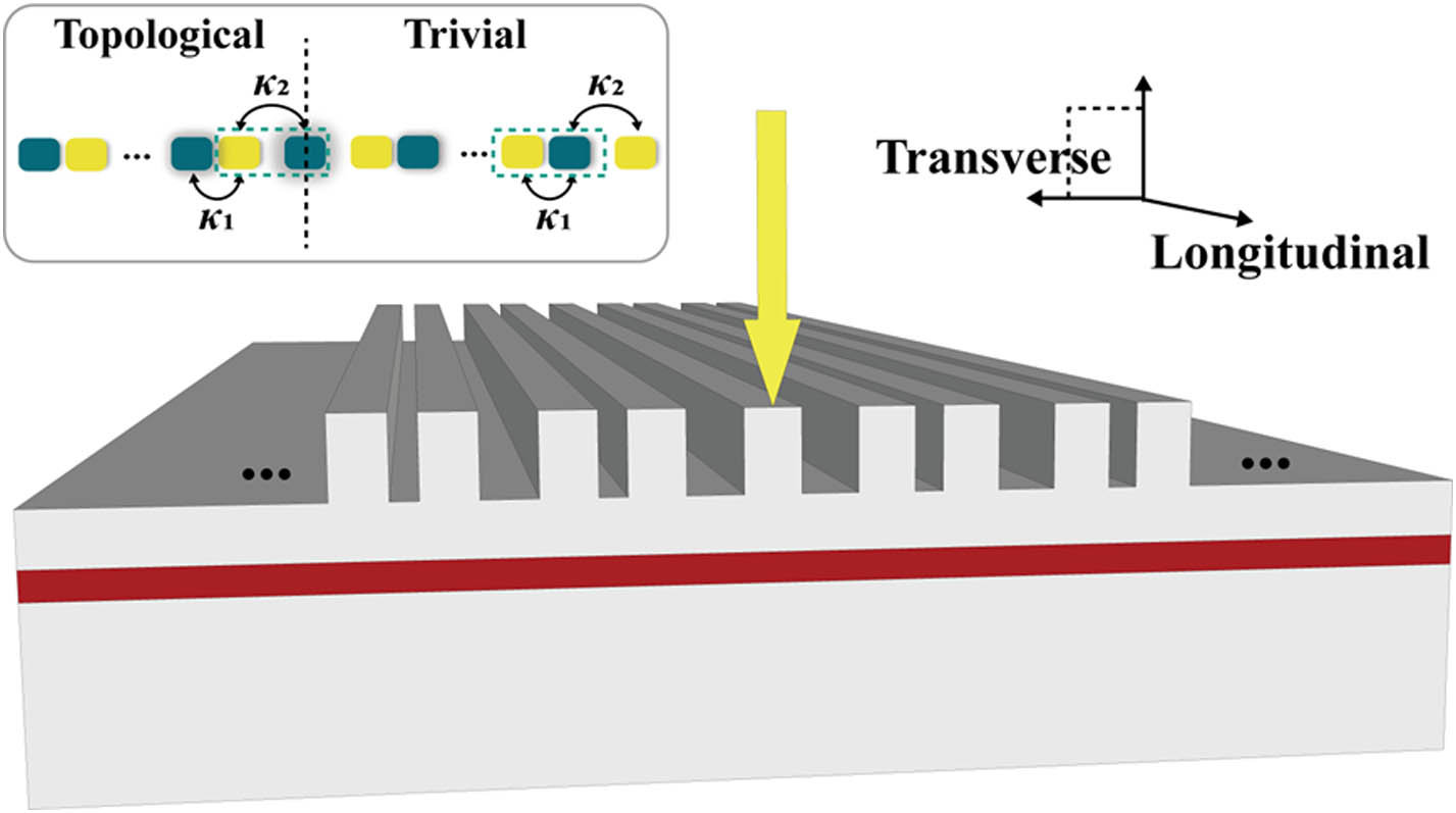
Figure 1.Schematic of the topological semiconductor laser array based on the traditional SSH model with a single defect. The yellow arrow denotes current injection on the single-defect waveguide, and the red part is the active region. The inset presents a sketch of the traditional 1D SSH dimer chain, where the green dashed squares indicate primitive cells in two distinct topological phases. In the topological chain, inter-cell coupling is stronger than intra-cell coupling, while intra-cell coupling is stronger in the trivial chain. A zero-energy topological state emerges at the interface indicated by the black dashed line.
![]()
Figure 2.Mode dispersions in the (a) topological laser array and (b) perturbed topological laser array based on the traditional SSH model. The inset in (b) presents the intensity distribution of the zero-energy topological state in the perturbed topological laser array (circled in red). Complex mode dispersions in the (c) topological laser array and (d) perturbed topological laser array based on the traditional SSH model, with a loss term
Chiral symmetry enables the design to be immune to off-diagonal disorders, which are perturbations on coupling strengths as shown in Eq. (1) [15,16,19]. Chiral symmetry is still held with the perturbations. Therefore, we deliberately introduce off-diagonal perturbations near the defect waveguide and verify the robustness of the device. For the four waveguides close to the central defect waveguide in the perturbed topological laser array, the spacing distances between neighboring waveguides are set to be 2.0 μm, corresponding to the coupling coefficient at
In both laser arrays, only the defect waveguides are injected with current as shown in Fig. 1, we introduce a
In experiments, we fabricate both laser arrays with and without off-diagonal perturbations, as shown in Fig. 3. The current injection windows are introduced at the central defect waveguides where the zero-energy state mainly resides, indicated by yellow arrows in Fig. 3. The dashed squares in Figs. 3(a) and 3(b) cover four waveguides, and the perturbations are introduced into their neighboring distances. The light–current (LI) characteristics and spectra of both laser arrays are measured, and the results are presented in Fig. 4.
![]()
Figure 3.Microscope images of parts of fabricated laser arrays from top view. (a) Top-view image of the topological laser array. (b) Top-view image of the perturbed topological laser array; dashed square denotes the introduced perturbations. Only the neighboring distances between the encircled four waveguides are changed. The injection windows are introduced at the central ridge waveguides (denoted by yellow arrows).
![]()
Figure 4.LI curves and spectra of the fabricated topological laser array and perturbed topological laser array. Thresholds (
The LI curves of two laser arrays coincide well with each other, as shown in Fig. 4(a). It can be inferred that the introduced perturbations do not affect the output power of the laser array in the first place. To avoid intrinsic nonlinear effects in semiconductor lasers [27] that deteriorate mode behaviors as theoretically predicted, we measure the spectra of laser arrays near thresholds. Figures 4(b) and 4(c) present the spectra of the laser array based on the traditional SSH model at 1.5 and 2.0 times threshold currents, respectively. Figures 4(d) and 4(e) show the spectra of the perturbed topological laser array at identical injection currents, accordingly. The longitudinal mode intervals are both around 0.7 nm [28] since the cavity lengths of two laser arrays are both 500 μm. There are several peaks with mode spacing at 0.7 nm, as shown in Figs. 4(b)–4(e), which implies that these peaks correspond to different longitudinal modes. The uniformity of longitudinal modes under different injection currents is poor, as no other mode selection mechanisms are introduced in the longitudinal axis, while the gain spectrum of quantum wells tends to shift towards the long wavelength and broaden under higher injection currents [29]. There are no distinguishable sidelobes in each peak in Figs. 4(b)–4(e), indicating that only one transverse mode lases in two laser arrays [28]. In addition, based on Figs. 2(c) and 2(d), the zero-energy state lases preferentially under current injection. Therefore, only the zero-energy state lases in both original and perturbed topological laser arrays in experiments. We can make the conclusion that the zero-energy state of the topological laser array is robust against the perturbations introduced into the coupling strengths.
3. MULTI-DEFECT TOPOLOGICAL LASER ARRAY BASED ON SSH MODEL
Based on the results above, we propose a new design that includes multi-defect waveguides at the interface and enlarges the mode volume of the zero-energy state. We introduce two more waveguides next to the central defect waveguide in the laser array presented in Fig. 1. The inserted waveguides possess identical propagation constants with the original defect waveguide since the widths and heights of them are identical. Hence, inserted waveguides introduce perturbations only on adjacent distances between them, which correspond to coupling coefficients, and the zero-energy state would be protected by the robustness of chiral symmetry.
Injection current is introduced to three-defect waveguides in the design, and remaining waveguide arrays on both sides are named as side arrays here. To exclude other supermodes of the three-defect waveguides from lasing and suppress them under current injection, we modulate the neighboring distances between three-defect waveguides cautiously. The lines in the left part of Fig. 5(a) are propagation constants of the supermodes of the three-defect waveguides in isolation with side arrays, solved by CMT. The dots in the right part of Fig. 5(a) are propagation constants of supermodes of the side arrays without consideration of the three-defect waveguides. The propagation constants of the supermodes of the three-defect waveguides, except for that of the zero-energy state, lie in the allowed bands of side arrays as shown in Fig. 5(a). Therefore, the electrical field distributions of supermodes in the allowed bands would extend to the side arrays effectively and suffer much optical loss when the three-defect waveguides are coupled with uninjected side arrays [30]. Only the zero-energy topological state, which lies in the bandgap, would be confined within the pumping region and experience optical gain in this manner. Consequently, the zero-energy state localizes in multi-defect waveguides, and the mode volume of it would be enlarged, compared to that of the traditional SSH model. In Fig. 5(a), for the three-defect waveguides, the distances between adjacent waveguides are 1.4 μm, corresponding to
![]()
Figure 5.(a) Mode dispersions of three-defect waveguides (left) and side arrays (right). (b) Mode dispersion of the proposed three-defect laser array that holds the zero-energy state with enlarged mode volume. The intensity distribution of the zero-energy topological state with enlarged mode volume (circled in red) is shown in the inset in the right corner. A schematic of the proposed laser array is plotted in the left corner, where the yellow arrows denote current injections introduced to three-defect waveguides. (c) Complex mode dispersion of the three-defect laser array with a loss term
To verify the theoretical prediction above, we fabricate a laser array based on the theoretical design experimentally. The injection current is introduced to three-defect waveguides simultaneously by selectively etching the insulator on top of the epitaxy. A normal laser array, which consists of three ridge waveguides possessing identical width, height, and adjacent distances with the three-defect waveguides in our design, is also fabricated. The difference between the normal laser array and three-defect topological laser array is that there are no side arrays in the former one. Hence, the pumping area of two laser arrays is identical, making them comparable under equal current injections. The threshold currents of three-defect topological and normal laser arrays are both around 50 mA. The spectra of both laser arrays are measured at 75 mA and 100 mA, corresponding to 1.5 and 2.0 times their threshold currents, respectively.
The measured spectra are presented in Fig. 6. There are many nonnegligible sidelobes in the peaks in Figs. 6(c) and 6(d) compared to those in Figs. 6(a) and 6(b), as shown in insets. Since the longitudinal mode interval is around 0.7 nm, small sidelobes in each peak indicate multiple transverse modes lasing in the normal laser array in Figs. 6(c) and 6(d). Therefore, it can be inferred that other supermodes introduced by extra pumped waveguides are filtered in the proposed design in Figs. 6(a) and 6(b), and the proposed design supports only the lasing of the zero-energy topological state as predicted in Fig. 5(c). The insets in Fig. 7 are the near-field patterns collected through a charge-coupled device (CCD) camera at the output facets of single-defect and three-defect topological laser arrays. The enlargement of the mode volume is clear in the proposed three-defect laser array in Fig. 7(b) compared to the single-defect laser array in Fig. 7(a).
![]()
Figure 6.(a), (b) Spectra of the proposed three-defect topological laser array. (c), (d) Spectra of the normal laser array. (a), (c) Measured at 75 mA, which is equal to
![]()
Figure 7.Horizontal far-field distribution of the (a) traditional single-defect topological laser array and (b) three-defect topological laser array at
Since the proposed three-defect topological laser array supports only the lasing of the zero-energy topological state with an enlarged mode volume, the output characteristics of the proposed design are optimized accordingly, compared to the traditional single-defect laser array. Output powers of these two laser arrays are 10.9 mW and 8.6 mW [shown in Fig. 4(a)] under working currents (
4. SUMMARY
In summary, we have proposed and demonstrated a new method to improve localized interfaces and enlarge the mode volume of topological states by virtue of the robustness originating from chiral symmetry in the SSH model. We demonstrate the robustness of the zero-energy topological state in the traditional SSH model on the platform of electrically injected semiconductor laser arrays. Based on the robustness against coupling strengths, i.e., off-diagonal disorders, extra defect waveguides are introduced and pumped in the proposed semiconductor laser array. The measured spectra and near-field patterns demonstrate the lasing of the zero-energy state with an enlarged mode volume. The output power, series resistance, and divergence in far-field patterns are optimized compared to that of the traditional single-defect laser array. We can also introduce more than two waveguides at the interface in the future to improve the topological interface and enlarge the mode volume of the zero-energy state further to establish a high-power and robust light source. The proposed method provides the insight that topological robustness is not only a favorable intrinsic characteristic but can also be utilized to optimize the topological interface and state itself. Our work can inspire more studies on the robustness and redistribution of topological states from semiconductor laser arrays to other platforms for broader applications such as robust light transporting.
Acknowledgment
Acknowledgment. Jingxuan Chen thanks Mr. Xiangdong Zhang from Nankai University for the discussion on the SSH model.
APPENDIX A: MATERIALS AND METHODS
The ridge waveguide arrays as arranged in this paper are obtained by the standard I-line photolithography process and inductively coupled plasma (ICP) etching on InP epitaxy. After the etching process, the insulator layer (


Set citation alerts for the article
Please enter your email address

© Copyright 2018-2021 | Chinese Laser Press. All Rights Reserved 沪ICP备15018463号-20