• Chinese Journal of Lasers
  • Vol. 51, Issue 7, 0701014 (2024)
Xiangyue Liu1, Zhe Zhang1、*, Li Jiang1, Hongxuan Song2, Dianxiang Yao1, Siyi Huang1, Wenjie Xu3, Tonglin Huo3, Hongjun Zhou3, Runze Qi1, Qiushi Huang1、**, Zhong Zhang1, and Zhanshan Wang1
Author Affiliations
  • 1Institute of Precision Optical Engineering, School of Physical Science and Engineering, Tongji University, Shanghai 200092, China
  • 2College of Sciences, Shanghai University, Shanghai 200444, China
  • 3National Synchrotron Radiation Laboratory, University of Science and Technology of China, Hefei 230029, Anhui , China
  • show less
    DOI: 10.3788/CJL231540 Cite this Article Set citation alerts
    Xiangyue Liu, Zhe Zhang, Li Jiang, Hongxuan Song, Dianxiang Yao, Siyi Huang, Wenjie Xu, Tonglin Huo, Hongjun Zhou, Runze Qi, Qiushi Huang, Zhong Zhang, Zhanshan Wang. Thickness Control and Thermal Stability of Large‐Diameter Mo/Si Multilayer Films for Extreme Ultraviolet Source[J]. Chinese Journal of Lasers, 2024, 51(7): 0701014 Copy Citation Text show less
    Experimental equipments. (a) Sputtering equipment; (b) annealing equipment
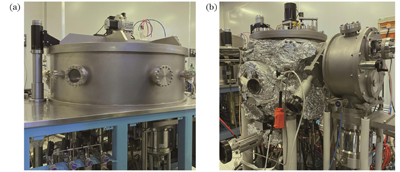
    Fig. 1. Experimental equipments. (a) Sputtering equipment; (b) annealing equipment
    Schematic of substituted substrate
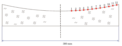
    Fig. 2. Schematic of substituted substrate
    Schematic of geometric relationship between substrate and shadow mask
    Fig. 3. Schematic of geometric relationship between substrate and shadow mask
    XRR measurement results of multilayer films at different positions on substituted substrate after film thickness correction using shadow mask
    Fig. 4. XRR measurement results of multilayer films at different positions on substituted substrate after film thickness correction using shadow mask
    AFM images of samples at different positions on curved substrate with 300 mm diameter. (a) X = 32.5 mm (sample 1); (b) X = 72.5 mm (sample 5); (c) X = 112.5 mm (sample 9); (d) X = 142.5 mm (sample 12)
    Fig. 5. AFM images of samples at different positions on curved substrate with 300 mm diameter. (a) X = 32.5 mm (sample 1); (b) X = 72.5 mm (sample 5); (c) X = 112.5 mm (sample 9); (d) X = 142.5 mm (sample 12)
    Normalized results for periodic thicknesses of samples at different positions on curved substrate with 300 mm diameter
    Fig. 6. Normalized results for periodic thicknesses of samples at different positions on curved substrate with 300 mm diameter
    XRR measurement results of multilayer film samples. (a) Mo/Si samples before and after annealing; (b) Mo/Si/C samples before and after annealing; (c) Mo/C/Si/C samples before and after annealing; (d) period thicknesses of Mo/Si, Mo/Si/C, and Mo/C/Si/C samples before and after annealing
    Fig. 7. XRR measurement results of multilayer film samples. (a) Mo/Si samples before and after annealing; (b) Mo/Si/C samples before and after annealing; (c) Mo/C/Si/C samples before and after annealing; (d) period thicknesses of Mo/Si, Mo/Si/C, and Mo/C/Si/C samples before and after annealing
    Measurement results of EUV reflectivity. (a) Mo/Si samples before and after annealing; (b) Mo/Si/C samples before and after annealing; (c) Mo/C/Si/C samples before and after annealing
    Fig. 8. Measurement results of EUV reflectivity. (a) Mo/Si samples before and after annealing; (b) Mo/Si/C samples before and after annealing; (c) Mo/C/Si/C samples before and after annealing
    TEM measurement results at different resolutions. (a) Mo/Si sample (low resolution); (b) Mo/C/Si/C sample (low resolution); (c) Mo/Si sample (high resolution); (d) Mo/C/Si/C sample (high resolution)
    Fig. 9. TEM measurement results at different resolutions. (a) Mo/Si sample (low resolution); (b) Mo/C/Si/C sample (low resolution); (c) Mo/Si sample (high resolution); (d) Mo/C/Si/C sample (high resolution)
    SampledMo /nmdC1 /nmdSi /nmdC2 /nm
    Mo/Si2.804.19
    Mo/Si/C2.603.880.48
    Mo/C/Si/C2.200.423.840.51
    Table 1. Multilayer film systems of annealed samples
    SampleTest contentBefore annealingAfter annealingVariation
    Mo/SiReflectivity64.4%55.4%-9.0%
    Central wavelength /nm13.4412.93-0.51
    Band width /nm0.460.35-0.11
    Mo/Si/CReflectivity66.4%59.6%-6.8%
    Central wavelength /nm13.4913.38-0.11
    Band width /nm0.490.45-0.04
    Mo/C/Si/CReflectivity65.2%63.4%-1.8%
    Central wavelength /nm13.6113.59-0.02
    Band width /nm0.490.50+0.01
    Table 2. EUV measurement results before and after annealing at 300 ℃ for 2 h
    Xiangyue Liu, Zhe Zhang, Li Jiang, Hongxuan Song, Dianxiang Yao, Siyi Huang, Wenjie Xu, Tonglin Huo, Hongjun Zhou, Runze Qi, Qiushi Huang, Zhong Zhang, Zhanshan Wang. Thickness Control and Thermal Stability of Large‐Diameter Mo/Si Multilayer Films for Extreme Ultraviolet Source[J]. Chinese Journal of Lasers, 2024, 51(7): 0701014
    Download Citation