
Huan Yuan, Zheqiang Zhong, Bin Zhang. Visible-frequency nonvolatile reconfigurable Janus metasurfaces for dual-wavelength-switched and spin-asymmetric holograms[J]. Photonics Research, 2024, 12(2): 356
- Photonics Research
- Vol. 12, Issue 2, 356 (2024)
Abstract
1. INTRODUCTION
In recent years, metasurfaces have garnered significant attention owing to their flexible manipulation of light and remarkable properties such as being ultralightweight and ultrathin [1–5]. Metasurfaces comprising artificially designed subwavelength units can provide a new paradigm for designing various ultracompact optical components. Owing to rapid advancements in micro-nano manufacturing and computer technologies, metasurfaces have been applied in various miniaturized optical fields, including holographic displays [6–9], optical encryption [10–15], nanoprinting [16–20], edge detection [21,22], diffraction neural networks [23,24], and optical stealth [25]. Deng
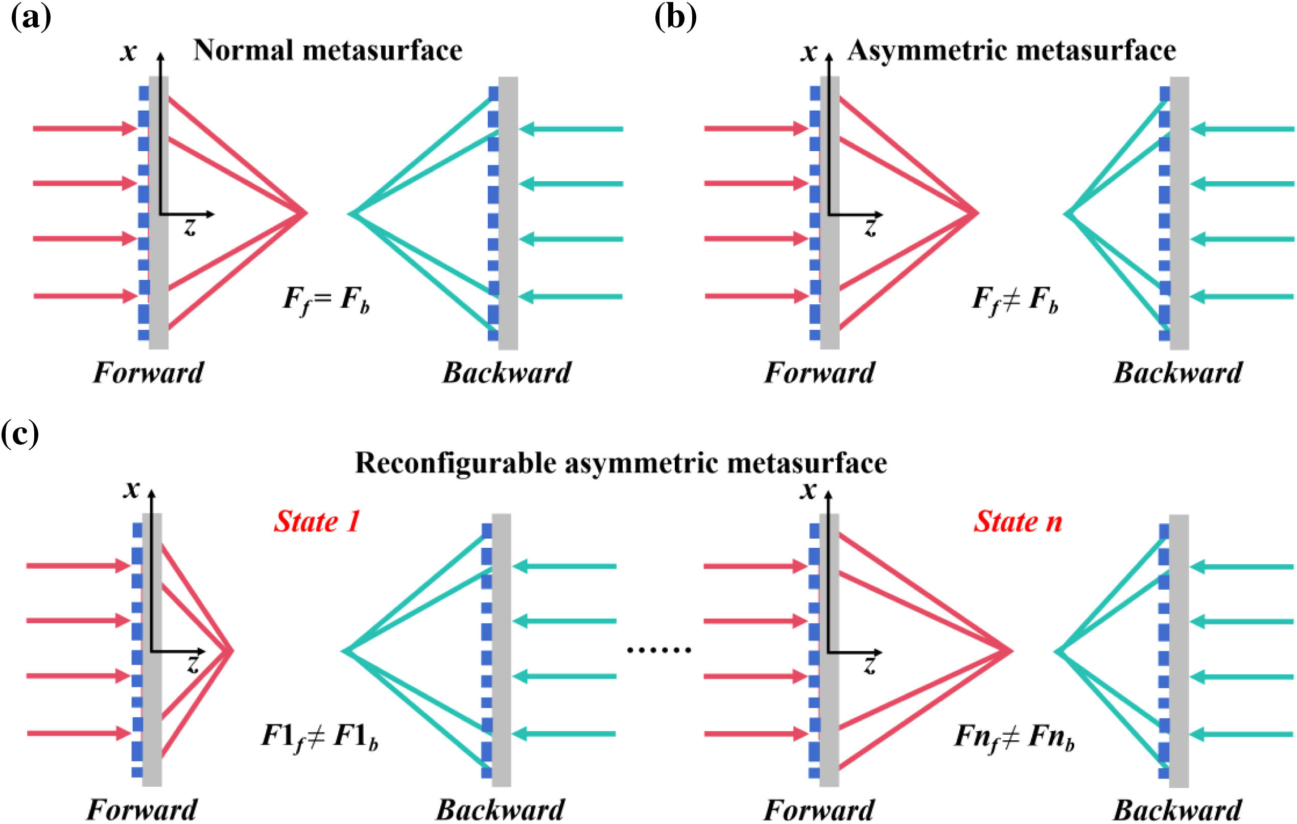
Figure 1.Schematic comparison of the optical functions of various types of metasurfaces. (a) Schematic diagram illustrating the transmission characteristics on both sides of a traditional transmissive metasurface (
A crucial property of electromagnetic waves, propagation direction, is often overlooked in comparison to commonly used parameters such as polarization, phase, incident angle, and wavelength. The Janus metasurface, which serves as a research platform for studying optical phenomena such as nonreciprocal transmission, can control the electromagnetic wavefront on both sides, enabling asymmetric reflection/transmission control [Fig. 1(b)] [28,29]. This metasurface has the potential to be a substitute for engineered multifunctional devices such as asymmetric metals and beam shaping [30,31]. However, traditional Janus metasurfaces rely heavily on complex multihierarchical structures, making them difficult to manufacture and expensive. To address these issues, single-layer metasurface structures based on both the propagation and geometric phases have been developed and utilized for asymmetric transmission [32–35]. For instance, Naveed
Fortunately, optical phase-change materials (O-PCMs) are highly desirable for designing tunable optical components owing to their reconfigurable properties [36–42]. O-PCMs typically exist in two primary states, crystalline and amorphous (insulated or metallic). The conversion between these two crystallinity states alters the arrangement of chemical bonds in the material, causing significant changes in its complex refractive index [43]. This enables the introduction of substantial phase and amplitude modulation in compact micro and nano sizes. The crystallinity of the O-PCMs can be altered by applying an external stimulus (such as light, electricity, or heat) [38,44,45], and the reversible switching between two stable states has a high durability of up to cycles [46]. However, classic O-PCMs such as alloys and exhibit high absorption losses at different crystallinity levels and cannot satisfy the requirements for high performance. Additionally, the volatility of limits its feasibility in the design of high-performance nonvolatile reconfigurable devices. For instance, Chen
Sign up for Photonics Research TOC. Get the latest issue of Photonics Research delivered right to you!Sign up now
![]()
Figure 2.Complex refractive indices,
In this study, we propose a novel nonvolatile reconfigurable single-layer Janus metasurface to achieve asymmetric wavefront generation and dynamically switched bidirectional holography. The Janus metasurface utilizes the reconfigurability of the nonvolatile O-PCM and the incident direction dependence. To design switchable asymmetric holograms on single-sized nanostructured metasurfaces, we developed a modified Gerchberg–Saxton (GS) algorithm by considering both the wavelength channels and propagation directions as the design objectives. In comparison with previous complex multilayer cascade designs, this reconfigurable metasurface can integrate multiple functions into a single phase-change element without introducing any additional loss, providing greater flexibility for regulating the light field. By changing the crystallinity of , these functions can be actively switched. In this study, we demonstrated a bidirectional asymmetric color-holographic display at three different crystallization levels. This scheme not only addresses the limitation of statically switching asymmetric holograms but also achieves multifunction integration on an ultrathin single-size nanostructure, significantly reducing manufacturing complexity and cost. The proposed scheme provides a versatile platform for information multiplexing and is promising for various practical applications, including mass data storage and optical encryption.
2. DESIGN AND METHODS
Figure 3(a) illustrates the concept of a switchable asymmetric hologram based on a nonvolatile reconfigurable Janus metasurface. The scheme allows for the integration of four independent holographic images onto a single metasurface. In the amorphous state, left-circularly polarized (LCP) light is incident forward and backward onto the metasurface, generating green hologram images of a portion of the “lion dance” and a portion of the “dragon” structure in the far field, respectively. In the crystalline state, red hologram images of another portion of the “lion dance” and “dragon” structures are generated in the far field, respectively. In the semi-crystalline state, LCP light is incident forward and backward onto the metasurface, generating complete color holographic images of the “lion dance” and “dragon” structures in the far field. The array, acting as meta-atoms on the metasurface, serves as a half-wave plate to convert circularly polarized (CP) light and enables asymmetric transmission of circularly polarized light. By utilizing the modified GS algorithm, the desired target function can be achieved by calculating the phase distribution on both sides of the metasurface and further arranging the orientation angles of the meta-atoms. Here, a single-phase profile of the meta-atoms array serves as the phase contribution function, encompassing the information required for different wavelength channels and transmission directions. The metasurface can switch between different functions by reversibly changing its crystalline and amorphous states as needed. Figure 3(b) illustrates the decoding keys required for decoding a holographic image and the associated optical properties for various key combinations.
![]()
Figure 3.Scheme for switching an asymmetric hologram based on a nonvolatile reconfigurable Janus metasurface. When LCP white light is incident onto the metasurface, either in a forward or backward direction, four independent holographic images are reconstructed under different states. (b) Left, three different optical decoding keys; right, optical characterization of the nonvolatile reconfigurable Janus metasurface.
To encode four different hologram images in the far field, we have developed a modified GS algorithm to determine the orientation angle of each meta-atom, as shown in Fig. 4. It is important to note that our geometric phase manipulation technique arises from the inherent property of the meta-atom, which provides two opposite phase distributions for both forward and backward incident CP light. Leveraging this property, we encode the desired phase onto the metasurface and reconstruct two different holographic images simply by changing the direction of incident light. Therefore, the design process of a multifunctional metasurface based on the modified GS algorithm can be divided into three steps [Fig. 4(a)]. (1) Using the GS algorithm, we design the phase required for forward image 1 and backward image 1 at the wavelength of 550 nm. The total geometric phase profile required is then calculated based on the phase merging formula. (2) Similarly, the GS algorithm is used to design the phase required for forward image 2 and backward image 2 at the wavelength of 650 nm. The total geometric phase profile required is then calculated based on the phase merging formula. When two beams of the same CP light are incident from opposite directions, the total geometric phase profile can be expressed as follows:
![]()
Figure 4.(a) Detailed flow chart of the reconfigurable asymmetric transmission metasurface design. (b) Optimization process using the modified GS algorithm.
The specific flow chart of this modified algorithm is depicted in Fig. 4(b). The intensity distributions of the four images are denoted as , , , and , respectively. The propagation process between the metasurface plane and the target plane is constructed using forward Fresnel diffraction (FFrD) and inverse Fresnel (IFrD) diffraction. The modified GS algorithm differs from the traditional one in that it considers both positive and negative values of the initial random phase before performing the Fresnel diffraction calculation. During the iterative process, the phase enhancement calculation is carried out according to Eqs. (1) and (2), simultaneously fulfilling the requirements of four-channel holographic images. After sufficient iterations, the optimized phase contours and are obtained. The distance between the metasurface and the two target planes is set as and , respectively. The propagation formulas for both FFrD and IFrD can be expressed as
To achieve this desired versatility, we have developed a novel single-layer metasurface structure that breaks symmetrical transmission. By optimizing the structural parameters of the meta-atom, we aimed to meet multiple requirements: (1) the spectral responses of meta-atoms should generate distinct colors in different states; (2) the transmission cross talk between different color channels should be minimized to prevent holographic image cross talk; (3) the circular polarization conversion efficiency should be maximized to ensure clear holographic images. To fulfill these requirements, we employed the particle swarm optimization (PSO) algorithm to optimize square nanorods. Here, we have taken 550 nm (green light) and 650 nm (red light) as the typical examples for the target wavelengths. Therefore, the target spectrum should exhibit narrowband filtering at both target wavelengths and a higher polarization conversion efficiency. The cell period of the elementary meta-atom is fixed at 380 nm (), as shown in Fig. 5(a). The optimized structural parameters include length , width , and height of the meta-atoms. It is worth noting that most O-PCMs have a high extinction coefficient in the visible region, which greatly limits their optical transmission efficiency. In our design, we utilize the nonvolatile O-PCM, , as the nanorods and optimize the structure size accordingly. The energy loss is effectively avoided in the visible region due to its low extinction coefficient (the complex refractive index at 633 nm: ; for visible light) (Fig. 2). The PSO algorithm yields the optimized structure parameters: , , and . Fortunately, these parameters are compatible with current advanced micro and nano machining technology. The transmission efficiency of the structure is simulated using the commercial software Lumerical finite-difference time-domain (FDTD) solutions. The intensity transmission curve for a single meta-atom under periodic boundary conditions is depicted in Fig. 5(b). The transmission spectrum of incident light can meet the functional requirements mentioned above when is in either its crystalline or amorphous state. Notably, both states exhibit distinct transmission peaks for LCP light at 550 nm and 650 nm, with peak polarization conversion efficiencies of 28.8% and 15.1%, respectively. Additionally, the cross-talk values for the two target wavelength channels are 0.65% and 1.03%, respectively. The cross talk between the two target wavelength channels is negligible. It is worth noting that the peak polarization conversion efficiency at a wavelength of 550 nm is higher than that at 660 nm, due to the lower extinction coefficient of compared to that of (see Fig. 2). To satisfy the required hologram phase, the PB phase principle is adopted to further select the orientation angle of the meta-atoms, assuming the identical sizes of the meta-atoms. The influence of the meta-atom’s orientation angle on the polarization conversion efficiency and PB phase in two states is shown in Fig. 5(c). The polarization conversion efficiency remains almost constant at the two target wavelengths, while the PB phase varies twice with the orientation angle (). Thus, the designed structure can meet the target function of the meta-atoms. The diffraction efficiency (DE), defined as the energy ratio between the transmitted and incident beam, is presented in Fig. 5(d) for various structural dimensions and , with a thickness of 500 nm. The spectral responses of cross-polarization transmittance in both states are converted into CIE 1931 color space chromaticity plots to quantitatively evaluate the obtained structural colors, as depicted by white solid dots in Fig. 5(e).
![]()
Figure 5.Structural design and optical properties of meta-atoms. (a) 3D view, side view, and top view of the meta-atom. (b) The transmissivity spectra of cross-polarization conversion are simulated at different levels of crystallization. (c) Cross-polarization transmission and phase variation are simulated at different crystallization levels with varying orientation angles. (d) The function of DE with
In Fig. 5(f), we utilized FDTD solutions to perform numerical calculations to demonstrate the independence of this meta-atom in two different states. By deliberately arranging a periodic array of meta-atoms with varying orientation angles, we intentionally create a complete gradient phase along the interface. This arrangement enables us to prove the abnormal refraction that occurs when two identical light beams are incident on the metasurface from the opposite sides. As shown in Fig. 5(f), in both states, when the same incident circularly-polarized light is incident on the metasurface from both sides, the outgoing light exhibits opposite beam steering phenomena. Consequently, the wavefronts of the incident light in both forward and backward directions confirm the desired asymmetric transmission performance.
Next, we employed this reconfigurable meta-atom to design a switchable Janus metasurface capable of generating direction-dependent, wavelength-dependent, and crystallinity-dependent holographic images in four channels. To achieve four independent holographic image channels on the metasurface, we utilized the meta-atoms as half-wave plates and rotated the orientation angle of meta-atoms by using geometric phase. Figure 6(a) provides an overview of the metasurface configuration, including top, zoomed, and angled views. The entire metasurface has a size of , and it consists of a total of meta-atoms. Figure 6(b) depicts the flow diagram of the reconstructed image using LCP light of different wavelengths. When is in the amorphous state, both forward and backward incident LCP green light passes through the metasurface, resulting in different encrypted images in the far field. Similarly, when is in the crystalline state, both forward and backward incident LCP red light passes through the metasurface, displaying different encrypted images in the far field. Lastly, when is in the semi-crystalline state, both green and red light, from the same forward and backward incidence, passes through the metasurface, generating different encrypted images with different colors in the far field. The reconfigurable Janus metasurface boasts a high level of encryption and exclusively retrieves the corresponding effective holographic image through the incidence of CP light. When using other types of light, such as linearly polarized light, only disordered and invalid image information can be observed. Furthermore, we calculated the broadband transmittance curve of the entire reconfigurable Janus metasurface. Figures 7(a) and 7(b) depict the transmission curves of the metasurface transmission terminal under different crystallinity conditions. The total cross-polarization transmission efficiency at 550 nm in the amorphous state reaches 26.3%, while the corresponding value at 650 nm in the amorphous state reaches 13.5%. Notably, the metasurface exhibits robust transmission performance when utilized for bidirectional dynamic holographic display.
![]()
Figure 6.(a) Diagram of the entire reconfigurable asymmetrical transmission metasurface configuration with top view, zoomed view, and angled view. (b) The flow chart of the image is reconstructed using different wavelengths of LCP light at various levels of crystallinity.
![]()
Figure 7.Co-polarization and cross-polarization transmission efficiency of the reconfigurable Janus metasurface sample with different crystallinity. (a)
The metasurface enables multichannel image encryption by encoding the incident direction, crystallinity, and wavelength. Figure 8 illustrates the decoding process using different optical keys. The holographic images on the left side of Figs. 8(a) and 8(d) are obtained through numerical calculations using the modified GS algorithm, with each cell containing a total of pixels. These images exhibit high-fidelity quality in different channels. Additionally, we employed the commercial software FDTD solutions to simulate the metasurface. Due to limited computation resources, the number of pixels was reduced to . The simulation results on the right side of Figs. 8(a) and 8(d) align with the predetermined dynamic multifunction design. The images encoded in different holographic channels are associated with the three optical keys mentioned above and can only be decoded using a specific combination of encoding. This novel holographic encryption scheme can significantly enhance information security and holds great potential for optical encryption application. Moreover, exhibits changes in multiple energy states during its transition from the amorphous state to the crystalline state, allowing the phase transition metasurface to be controlled by a multilevel wavefront. The dielectric constant of the intermediate phases of can be calculated using the Lorenz–Lorentz relation [48]:
![]()
Figure 8.(a) Simulation results of a single wavelength LCP incident light with a wavelength of 550 nm (650 nm) when the metasurface is in an amorphous (crystalline) state. (b) Complex refractive index curve of the semi-crystalline
To address the manufacturing tolerances of this reconfigurable Janus metasurface, we conducted simulations to assess the effects of varying the length, width, and thickness of the top nanorods on the cross-polarized transmission spectrum, as depicted in Fig. 9. Figures 9(a)–9(c) illustrate the impact of different structural parameters including the width, length, and thickness of nanorods on the efficiency of cross-polarization conversion. In each figure, the peak transmission offset is represented by a black dashed line. Furthermore, Figs. 9(d)–9(f) illustrate the impact of different width, length, and thickness of nanorods on the efficiency of cross-polarization conversion. Figure 9 implies that the reconfigurable Janus metasurface can still maintain good performance within a certain range of structural size.
![]()
Figure 9.Manufacturing tolerances of the reconfigurable Janus metasurface. (a) Variation of the simulated cross-polarization transmission spectra of
3. CONCLUSIONS
In summary, we demonstrated the use of a reconfigurable Janus metasurface based on single-sized nanostructures for dynamic switching displays without the need for complex and difficult manufacturing processes. In addition, we proposed a modified holographic optimization strategy to achieve high-fidelity asymmetric holographic imaging. The mechanism underlying this approach combines the geometric phase and crystallinity transitions, resulting in different optical responses to the same CP light when incident from opposite directions. In the visible region, we realized a color-holographic encryption display of wavelength, incident direction, and crystal state using an O-PCM array, which was previously impossible with asymmetric transmission metasurfaces. The results demonstrate that the display of different color holographic patterns can be independently controlled by switching three keys: wavelength, incident direction, and crystal state. Furthermore, by combining this scheme with deep learning methods or other optimization algorithms, the number of image channels encoded within a single metasurface can be further increased. With the advantages of miniaturization, integration, and tunability, reconfigurable metasurfaces hold significant potential for application in next-generation color-optical encryption elements.
APPENDIX A: PARAMETERS OF SELECTED NANOBRICKS
The transmittance of meta-atoms with varying sizes ( and ranging from 50 to 160 nm) was simulated at different wavelengths, crystallinity, and polarization states by using FDTD solutions, as shown in Fig.
![]()
Figure 10.Numerical analysis of unit structures for reconfigurable asymmetric transmittance metasurfaces. The scanning results are separately calculated for different wavelengths, levels of crystallinity, and polarization states.
APPENDIX B
To achieve nanorods with excellent narrowband filtering characteristics, the introduction of intelligent algorithms for optimal design is necessary. We utilized the particle swarm optimization algorithm to optimize the size of the structure, as depicted in Fig.
![]()
Figure 11.Design process of the PSO algorithm for optimizing the size of the nanorods.
APPENDIX C
The versatile wave manipulation capabilities of asymmetric transmission metasurfaces make them highly attractive for applications in information encryption and storage. In recent years, significant research efforts have focused on enhancing the information processing capabilities of metasurface holograms through asymmetric transmission. Table Comparison between Our Work and Other Reported WorksRefs. [ [ [ [ This work Material Cu, dielectric substrates a-Si:H, a-Si, Au, polyimide, Target wavelength 8.6 GHz 632.8 nm 663 nm 0.99 THz 550 nm, 650 nm Structure mode Three layers cascade Single layer Single layer Three layers cascade Single layer Asymmetric transmission √ √ √ √ √ Reconfigurable × × × √ √ Nonvolatile × × × × √ Decoding key Direction of propagation Direction of propagation Direction of propagation Direction of propagation, crystallinity Direction of propagation, crystallinity, wavelength Number of channels 2 2 2 4 6
APPENDIX D
The potential manufacturing steps for the proposed reconfigurable Janus metasurface are depicted in Fig.
![]()
Figure 12.Potential manufacturing steps for the reconfigurable Janus metasurface.
APPENDIX E
To characterize the optical properties of our reconfigurable Janus metasurface, we proposed a holographic imaging device for the visible spectrum under CP light incident conditions, as shown in Fig.
![]()
Figure 13.Potential experimental setup for measuring the encrypted holographic images.
References
[4] N. Yu, F. Capasso. Flat optics with designer metasurfaces. Nat. Mater., 13, 139-150(2014).
[28] K. Chen, G. Ding, G. Hu. Directional Janus metasurface. Adv. Mater., 32, 1906352(2019).
[46] O. Hemmatyar, S. Abdollahramezani, I. Zeimpekis. Advanced phase-change materials for enhanced meta-displays. arXiv(2021).

Set citation alerts for the article
Please enter your email address
© Copyright 2018-2021 | Chinese Laser Press. All Rights Reserved 沪ICP备15018463号-20