
Xuyang Wang, Yanxiang Jia, Xubo Guo, Jianqiang Liu, Shaofeng Wang, Wenyuan Liu, Fangyuan Sun, Jun Zou, Yongmin Li. Silicon photonics integrated dynamic polarization controller[J]. Chinese Optics Letters, 2022, 20(4): 041301
- Chinese Optics Letters
- Vol. 20, Issue 4, 041301 (2022)
Abstract
Keywords
1. Introduction
The dynamic polarization controller (DPC) is a crucial component in fiber optic communication[
Several promising platforms on integrated optic polarization controllers have been reported[
In this work, we design and demonstrate a full silicon photonics integrated DPC. By employing the variable step simulated annealing approach, we achieve a dynamic polarization extinction ratio greater than 25 dB. The experimental results agree well with theoretical simulation. The performance of the compact silicon photonics integrated polarization controller is close to that of the commercial fiber DPC. The overall size of the DPC on chip was , which was much smaller than that of fiber-squeezers-based DPC.
Sign up for Chinese Optics Letters TOC. Get the latest issue of Chinese Optics Letters delivered right to you!Sign up now
In Section 2, the design of the silicon photonics integrated DPC is presented. In Section 3, the characters of the thermal phase shifters (TPSs) are evaluated. There is good linearity between the phase shift and the power consumed by the metal heater. The modulation bandwidth is about 30 kHz. In Section 4, we present the numerical simulation and experimental results of the silicon photonics integrated DPC. The advantages of the variable step simulated annealing approach are demonstrated, and a dynamic polarization extinction ratio larger than 25 dB is obtained. Finally, Section 5 presents the ways to improve the performance of the DPC and the conclusions.
2. Design of Silicon Photonics Integrated DPC
Generally, the DPC comprising three or four fiber squeezers was utilized in fiber communication systems. The fiber squeezers were activated by piezoceramic actuators, which were driven by the high voltage of above 100 V. The squeezers alternated between 0°, 45°, 0°, and 45° of orientation. Each squeezer introduced a phase shift between the linear polarization components aligned parallel and perpendicular to the squeezing direction. The phase shift can be varied by altering the squeezing force. The fiber under the stress can be represented in Jones calculus by two kinds of transformation matrices and , as indicated in Eq. (1):
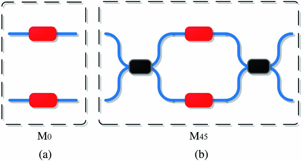
The transformation matrices can be transformed into the corresponding structures of silicon photonics integrated circuits, as demonstrated in Fig. 1[
![]()
Figure 1.Structures of silicon photonics integrated circuits corresponding to the transformation matrices M0 and M45. (a) The structure corresponds to matrix M0; (b) the structure corresponds to matrix M45.
According to the above basic structures, the DPC consisting of silicon photonics integrated circuits was designed, as indicated in Fig. 2(a). The input and output ports were 2D grating couplers (GCs) that were utilized as the polarization beam splitter (PBS)[
![]()
Figure 2.Structure and photograph of silicon photonics integrated DPC. PD, photodiode. (a) The structure of the DPC; (b) the photograph of the DPC.
Figure 2(b) indicates the photograph of silicon photonics integrated DPC. The fabrication of the device was performed with CSiP180Al active flow technology. It was based on a 200 mm SOI substrate with 2 µm buried oxide (BOX) and 220 nm top silicon. The overall size of the DPC was , which was much smaller than that of the fiber-squeezers-based DPC with the size of (PolaRITE III, GP). Here, TPS was employed to alter the delayed phase. The 25 µm golden wire was selected to bond the pad by which the driving voltage can be applied on the DPC. The characters of the TPS are evaluated in detail in the next section.
3. Characterization of the TPS
The characters of the TPS or TiN metal heater are evaluated utilizing a Mach–Zehnder (MZ) modulator. The length of the TPS is 400 µm, and the resistance of the metal heater is 1.97 kΩ. A 1 mW 1550 nm continuous laser beam was coupled into one port of the MZ modulator. By varying the voltage on the metal heater of one side, the output power was altered. We transformed the voltage into the power applied on the metal heater utilizing the expression
As shown in Fig. 3(a), there is a good linearity between the phase shift and the power consumed by the metal heater. The total phase shift is roughly by varying the power from 0 to 50.56 mW, which corresponds to the applied voltage from 0 to 10 V. The phase shift amount is enough to stabilize the polarization with the simulated annealing method. Note that many digital-to-analog converter chips’ output voltages can reach this voltage, and a high voltage amplifier is unnecessary. In contrast, the voltage of 140 V is required to drive the piezo of PolaRITE III.
![]()
Figure 3.Characterization of the TPS. (a) The phase shift versus the consumed power of the thermal heater; (b) the rise and fall time of the MZ modulator.
In addition, the modulation speed of the phase was evaluated, which determines the polarization locking speed. In the measurement, a 40 µs electronic square pulse with a peak voltage of 5.6 V was applied to the metal heater of the MZ modulator. It corresponds to a phase shift of . The rising time was measured to be 11 µs, and the falling time is 5.9 µs. This value is about one-tenth of the rise time of PolaRITE III. Thus, the modulation bandwidth is about 30 kHz.
4. Numerical Simulation and Experimental Results
The simulated annealing approach is a good approach to lock the output SOP. Usually, a big step is needed to realize high-speed polarization controlling. However, from the simulation, we discovered that to obtain a higher polarization extinction ratio, a small step is necessary. To address this issue, the variable step approach was adopted to increase the speed and extinction ratio of the SOP locking simultaneously. The flow chart of the program is illustrated in Fig. 4.
![]()
Figure 4.Flow chart of the variable step simulated annealing method.
We started by setting the initial temperature as . The variable is used to count the external loops, and the number of the total loops is in a round. The variable is used to count the internal loops, and the number of the total loops is in an external loop. There are totally 500 internal loops in a round. The maximal intensity of the input beam is normalized. Then, we set the initial value of the four delay phases to and stored them into an array . Then, we calculated the output intensity according to the delay phases and the SOP of the input beam. Here, denotes the intensity of the beam from one output port of the PBS followings the DPC. and denote the maximum intensity of and corresponding delayed phases, respectively. denotes the intensity of the beam from the other output port of the PBS.
Before entering the external loop, the value was initialized to one, and the value was initialized to . In the external loop, the temperature decreases with the proportion function:
The simulation results are shown in Fig. 5. The fixed step method with two different steps and the variable step method were compared. When the step was larger (), the required internal loops were less. However, the extinction ratio is lower. For a smaller step of , a higher extinction ratio can be obtained at the cost of more internal loops to reach the steady value. It is obvious that the best result is achieved by the variable step simulated annealing methods, where the highest extinction ratio is obtained with the least internal loops.
![]()
Figure 5.Simulation results of dynamic polarization control. It represents the extinction ratio versus the number of the internal loops with fixed and variable step simulated annealing methods. The noise and static polarization extinction ratio were considered. N, noise; SPER, static polarization extinction ratio.
Note that the static polarization extinction ratio, electronic noises of the photodetectors, and fluctuations of the optical power determine the ultimate limit of the DPC. In the simulation, the minimum intensity of is set to , considering the statistic polarization extinction ratio of the 2D GC of 28 dB. The standard variance of the electronic noises and optical power fluctuation is set to (normalized to the maximum intensity of one).
The scheme of the test setup is illustrated in Fig. 6. A 1550 nm fiber pigtailed DFB laser was utilized to generate a continuous beam, and a variable optical attenuator is used to tune the intensity of the laser beam. Part of the beam, which was employed to monitor the laser power, was separated by a 50/50 fiber SM coupler. An MPC is employed to tune the SOP of the beam directed into the chip. An alignment machine was utilized to align the fiber to the top of the 2D GC nearly vertically with an angle of 80°. The power coupled into the chip is 1 mW. The measured total loss from the input 2D GC to the output 2D GC is . The coupling loss of the fabricated 2D GC is 7 dB. Considering the 3 dB loss from the 50/50 MMI on the chip, the transmission loss of the integrated DPC is 3 dB, which mainly originates from the four MMIs. After transmitting through the chip, the beam was directed into the SM fiber again. Then, it was separated by the fiber PBS into path 1 and path 2. The intensity of the beam in the paths was evaluated by detector 1 and detector 2. The DPC on the chip is exploited to maximize the intensity of the beam in path 1 (detector 1), and, therefore, the intensity of the beam in path 2 (detector 2) is minimized.
![]()
Figure 6.Experimental setup to test the silicon photonics integrated DPC. MPC, manual polarization controller; MF, multifunctional.
Based on the simulation results, we employed the variable step approach to lock the SOP of the laser. The output voltage limit of the multifunction input/output (I/O) card was 10 V. From Section 3, this voltage range can result in a phase shift of . This phase shift range is enough to lock the SOP by setting the initial phase shift at . By fitting the experiment results in Fig. 3(a), a linear formula can be obtained as follows:
From Eq. (8), we observe that decreases with the voltage for a constant . When the value of voltage is small, the voltage step will be very large. The minimum value corresponds to the maximum value of , and it is not relevant to . In our experiment, was used to ensure more stable polarization control for the corresponding or st value.
The experiment results of our silicon photonics integrated dynamic polarization controlling are shown in Fig. 7. Before the operation of the DPC control procedure, the voltage of detector 2 was set to the maximum value by the MPC. For the measurement range of detector 2, its output was saturated at the beginning of the DPC control. The black line represents the results utilizing a fixed step of 0.005 V (0.008 rad at ) with internal loops. The red line represents the results utilizing a fixed step of 0.1 V (0.16 rad at ) with internal loops. The blue line represents the results utilizing a variable step. For the variable step approach, a extinction ratio higher than 25 dB is obtained with internal loops. This value is nearly close to the static extinction ratio of 28 dB of our silicon photonics integrated DPC. The experimental results are similar to the simulation results in Fig. 5. To achieve a better dynamic polarization extinction ratio in experiment, a low noise photodetector should be utilized, and multiple samples were averaged to minimize the electronic noise and optical power fluctuation.
![]()
Figure 7.Experiment results of dynamic polarization control. It represents the extinction ratio versus the number of internal loops with fixed and variable step simulated annealing methods.
5. Discussion and Conclusions
For further study, it is very promising to decrease the coupling efficiency of the silicon photonics integrated DPC from 7 dB to 2 dB or less by using the butting coupling method with an appropriate spot size converter between the on-chip silicon waveguide and SM fiber. On the SM fiber side, a fiber lens or large numerical aperture optical fiber is recommended. On the integrated DPC side, the spot size converter and polarization rotator-splitter should be used to replace the 2D GC[
The modulation bandwidth of the DPC designed by us is about 30 kHz. Considering the voltage of 5.6 V applied on the TPS, the bandwidth-voltage product is . Therefore, the bandwidth-voltage product is much higher than the commercial product based on squeezing the fiber (PolaRITE III with driving board PCD - M02), which has a typical value of 1.25 kHz·V. More importantly, the high voltage about 140 V is no longer needed. Considering that a faster modulation speed is needed in some cases, the P-I-N phase shifter based on the plasma dispersion effect of silicon can be used to replace the TPS. The modulation bandwidth of tens of MHz or higher can be achieved. However, the insertion loss of the P-I-N phase shifter is higher, and the loss increases with the phase shift amount. This will affect the balance of the two arms and decrease the polarization extinction ratio of the DPC. Typically, for a 500 µm long P-I-N phase shifter, the insertion loss is about 0.5–1 dB or even smaller. The excess insertion loss is 0.1–0.2 dB when the phase shift amount is , and the excess insertion loss is 0.5–1 dB when the phase shift amount is .
Compared with the polarization controllers based on silicon photonics integrated circuits[
In conclusion, we have designed and demonstrated a compact silicon photonics integrated DPC. The structures and principles of operation were presented in detail. A polarization extinction ratio higher than 25 dB was achieved with the variable step simulated annealing approach. Numerical simulation was used to optimize the experimental parameters. The methods to decrease the loss and increase the modulation speed for the device are also discussed. With the butting coupling method and polarization rotator-splitter, the effective transmission loss will be significantly reduced, resulting in a better transmission performance of fiber communication systems. It is expected that the device can also find applications in silicon photonics integrated QKD systems.
References
[1] D. X. Dai, C. L. Li, S. P. Wang, H. Wu, Y. C. Shi, Z. H. Wu, S. M. Gao, T. G. Dai, H. Yu, H. K. Tsang. 10-channel mode (de)multiplexer with dual polarizations. Laser Photon Rev., 12, 1700109(2018).
[2] J. Wang, S. L. He, D. X. Dai. 10-channel mode (de)multiplexer with dual polarizations. Laser Photon Rev., 8, L18(2018).
[3] Z. Y. Chen, L. S. Yan, Y. Pan, L. Jiang, A. L. Yi, W. Pan, B. Luo. Use of polarization freedom beyond polarization-division multiplexing to support high-speed and spectral-efficient data transmission. Light Sci. Appl., 6, e16207(2017).
[4] J. S. Tyo, D. L. Goldstein, D. B. Chenault, J. A. Shaw. Review of passive imaging polarimetry for remote sensing applications. Appl. Opt., 45, 5453(2006).
[5] D. S. Ding, W. Zhang, Z. Y. Zhou, S. Shi, B.-S. Shi, G. C. Guo. Raman quantum memory of photonic polarized entanglement. Nat. Photonics, 9, 332(2015).
[6] P. Jouguet, S. Kunz-Jacques, A. Leverrier, P. Grangier, E. Diamanti. Experimental demonstration of long-distance continuous-variable quantum key distribution. Nat. Photonics, 7, 378(2013).
[7] J. W. Wang, F. Sciarrino, A. Laing, M. G. Thompson. Integrated photonic quantum technologies. Nat. Photonics, 14, 273(2020).
[8] X. Y. Wang, W. Y. Liu, P. Wang, Y. M. Li. Experimental study on all-fiber-based unidimensional continuous-variable quantum key distribution. Phys. Rev. A, 95, 062330(2017).
[9] Y. C. Zhang, Z. Y. Chen, S. Pirandola, X. Y. Wang, C. Zhou, B. J. Chu, Y. J. Zhao, B. J. Xu, S. Yu, H. Guo. Long-distance continuous-variable quantum key distribution over 202.81 km of fiber. Phys. Rev. Lett., 125, 010502(2020).
[10] E. Diamanti, H. K. Lo, B. Qi, Z. Yuan. Practical challenges in quantum key distribution. NPJ Quant. Inf., 2, 16025(2016).
[11] G. F. Xin, L. Shen, H. Y. Pi, D. J. Chen, H. W. Cai, H. Z. Feng, J. X. Geng, R. H. Qu, G. T. Chen, Z. J. Fang, W. B. Chen. Polarization-locked VCSEL with PM fiber pigtail for quantum communication. Chin. Opt. Lett., 10, 101403(2012).
[12] P. Y. Zhang, L. L. Lu, F. C. Qu, X. H. Jiang, X. D. Zheng, Y. Q. Lu, S. N. Zhu, X. S. Ma. High-quality quantum process tomography of time-bin qubit’s transmission over a metropolitan fiber network and its application. Chin. Opt. Lett., 18, 082701(2020).
[13] K. Wei, W. Li, H. Tan, Y. Li, H. Min, W. J. Zhang, H. Li, L. X. You, Z. Wang, X. Jiang, T. Y. Chen, S. K. Liao, C. Z. Peng, F. H. Xu, J. W. Pan. High-speed measurement-device-independent quantum key distribution with integrated silicon photonics. Phys. Rev. X, 10, 031030(2020).
[14] C. X. Ma, W. D. Sacher, Z. Y. Tang, J. C. Mikkelsen, Y. Yang, F. H. Xu, T. Thiessen, H. K. Lo, J. K. S. Poon. Silicon photonic transmitter for polarization-encoded quantum key distribution. Optica, 3, 1274(2020).
[15] P. Sibson, J. E. Kennard, S. Stanisic, C. Erven, J. L. O’Brien, M. G. Thompson. Integrated silicon photonics for high-speed quantum key distribution. Optica, 4, 172(2017).
[16] P. Sibson, C. Erven, M. Godfrey, S. Miki, T. Yamashita, M. Fujiwara, M. Sasaki, H. Terai, M. G. Tanner, C. M. Natarajan, R. H. Hadfield, J. L. O’Brien, M. G. Thompson. Chip-based quantum key distribution. Nat. Commun., 8, 13984(2017).
[17] G. Zhang, J. Y. Haw, H. Cai, F. Xu, S. M. Assad, J. F. Fitzsimons, X. Zhou, Y. Zhang, S. Yu, J. Wu, W. Ser, L. C. Kwek, A. Q. Liu. An integrated silicon photonic chip platform for continuous-variable quantum key distribution. Nat. Photonics, 13, 839(2019).
[18] J. D. Sarmiento-Merenguel, R. Halir, X. Le Roux, C. Alonso-Ramos, L. Vivien, P. Cheben, E. Durán-Valdeiglesias, I. Molina-Fernández, D. Marris-Morini, D. X. Xu, J. H. Schmid. Demonstration of integrated polarization control with a 40 dB range in extinction ratio. Optica, 2, 1019(2015).
[19] J. W. Kim, S. H. Park, W. S. Chu, M. C. Oh. Integrated-optic polarization controllers incorporating polymer waveguide birefringence modulators. Opt. Express, 20, 12443(2012).
[20] H. L. Zhou, Y. H. Zhao, Y. X. Wei, F. Li, J. J. Dong, X. L. Zhang. All-in-one silicon photonic polarization processor. Nano Photonics, 8, 2257(2019).
[21] P. Velha, V. Sorianello, M. V. Preite, G. De Angelis, T. Cassese, A. Bianchi, F. Testa, M. Romagnoli. Wide-band polarization controller for Si photonic integrated circuits. Opt. Lett., 41, 5656(2016).
[22] L. Moller. WDM polarization controller in PLC technology. IEEE Photon. Technol. Lett., 13, 585(2001).
[23] J. Zou, Y. Yu, X. L. Zhang. Two-dimensional grating coupler with a low polarization dependent loss of 0.25 dB covering the C-band. Opt. Lett., 41, 4206(2016).
[24] J. Zou, X. Ma, X. Xia, C. H. Wang, M. Zhang, J. H. Hu, X. Y. Wang, J. J. He. Novel wavelength multiplexer using (N + 1) × (N + 1) arrayed waveguide grating and polarization-combiner-rotator on SOI platform. J. Lightwave Technol., 39, 2431(2021).

Set citation alerts for the article
Please enter your email address
© Copyright 2018-2021 | Chinese Laser Press. All Rights Reserved 沪ICP备15018463号-20