
Rui Shao, Gong Zhang, Xiao Gong, "Generalized robust training scheme using genetic algorithm for optical neural networks with imprecise components," Photonics Res. 10, 1868 (2022)
- Photonics Research
- Vol. 10, Issue 8, 1868 (2022)
Abstract
1. INTRODUCTION
Implementation of neuromorphic photonics on a silicon photonic integrated chip is gradually becoming a promising technology for deep learning accelerators, which utilizes photonic processors to function as artificial intelligence (AI) cores [1–4]. The realization and advancement of integrated programmable photonic processors [5–13] provide a feasible strategy for the construction of optical neural networks (ONNs) [14,15]. Compared to electronics, neuromorphic photonics has advantages of well-known high-bandwidth, and ultralow energy consumption due to negligible energy for light propagation with encoded information [16]. With the rapid advancement of the complementary metal–oxide–semiconductor (CMOS)-compatible silicon-on-insulator (SOI) platform [17–19], integrated silicon waveguides [20] and optical modulators such as Mach–Zehnder interferometers (MZIs) [21–26] and micro-ring resonators (MRRs) [27–29] can be easily formed as programmable processors for the construction of integrated ONNs [21,22,30,31] and other similar deep learning networks such as convolutional neural networks (CNNs) [6,32,33] and recurrent neural networks (RNNs) [2,34].
However, there remain challenges in the precise control of device performance and achieving excellent uniformity for various components in neuromorphic photonic chips. For example, there is a 15% reduction of vowel classification accuracy with the nanophotonic processor [22] and limited accuracy (about 88%) in handwriting image recognition using the photonic CNN chip [33]. The major problem is non-ideal photonic components, which leads to uncertain performance of the required functionality. In previous research, a few optimization procedures have been reported aiming at restoring the fidelity of the unitary matrix by using numerical initialization of parameters in MZIs [35,36]. However, these strategies mainly focused on the fidelity of the implemented unitary matrix instead of the desired functionality of the ONN. Hence, the effects of imprecise components could be underestimated. Also, these optimizations require precise characterization of each device separately and are actualized after fabrication, leading to extra computational power consumption and suffering from scalability problems in mass production.
Other methods adopted physical architecture modification to mitigate the effects of imprecisions. A double MZI configuration was proposed to compensate for fabricated MZIs with imperfect splitting ratios without calibration [37]. Shokraneh et al. [38] reported a diamond mesh of MZIs, which forms a symmetrical architecture to resist imprecisions in the ONN, and Fang
Sign up for Photonics Research TOC. Get the latest issue of Photonics Research delivered right to you!Sign up now
To address the above-mentioned issues, in this paper, we propose a two-step
We perform the training scheme in a feedforward photonic neural network implemented by the mesh of MZIs with tunable thermo-optic phase shifters and demonstrate its effectiveness in practical learning tasks, including
2. ONN ARCHITECTURE AND TRAINING SCHEME
A. Constructions of ONN
The typical ONN is a feedforward sequential processing flow comprising an input layer with artificial neurons, a series of hidden layers, activation layers, and an output layer, as shown in Fig. 1(a). The continuous wave laser source and optical amplifier generate an optical signal and split it into different waveguide channels. The input image is encoded into the optical signal in the form of
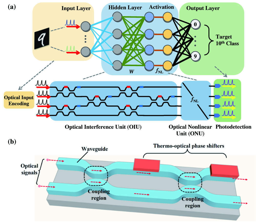
Figure 1.(a) Illustration of artificial neural network (ANN) architecture for image recognition implemented by photonic units, including optical input encoding parts, optical interference units, optical nonlinear units, and photodetectors. (b) Demonstration of a programmable Mach–Zehnder interferometer consisting of directional couplers and thermo-optical phase shifters.
The paramount part in the ONN to function as the synaptic weight
B. Quantized Parameter Imprecisions
Since there are severe impacts of parameter imprecisions, the distorted scattering matrix of the MZI caused by these errors is consequently obtained. There are four main types of imprecisions in devices, including phase shift error, insertion loss, drift of the coupling coefficient, and photodetection noise. From previous experimental measurements [22], the phase errors
Another error in the MZI is insertion loss
Typically, after the optical–electrical conversion, there is photodetection noise
There are also other potential drifts existing in experiments, including optical input encoding, device aging, temperature, and learning duration. In the practical MZI-based ONN chip [21,22,31],
By using the quantized parameter imprecisions, the degradation of ONN performance can be directly evaluated on the basis of the network’s accuracy in the specific dataset. Distorted scattering matrices of the MZI array were set as synaptic weights in hidden layers. Then the imprecise ONN was applied to perform a machine learning task in the supervised learning way. Classification accuracy of the affected ONN in different error ranges was obtained as depicted in Fig. 2. Figure 2(a) demonstrates the accuracy degradation caused by phase shift error and MZI loss. The typical phase shift error is about 0.05 rad, which lowers the classification accuracy by about 4%. For silicon photonics, the loss of each MZI is about 0.05–0.1 dB, which indicates that the accuracy would drop by about 1%. Figures 2(b) and 2(c) indicate the impacts of the extinction ratio and photodetection noise on accuracy, respectively. The extinction ratio of experimentally measured MZI can reach 20 dB and photodetection noise about 0.05, reducing the accuracy by about 11% and 0.7%, respectively. This indicates that in practical cases, the coupling ratio error would contribute more to accuracy degradation than MZI loss or photodetection noise.
![]()
Figure 2.Heat map of classification accuracy in the MNIST dataset with the imprecise ONN chip. (a) Classification performance between phase shift error
C. Workflow of the Training Scheme
Without any calibration steps or extra imprecise network training, the ONN is typically sensitive to parameter imprecisions, hindering the use of photonic chips in machine learning. Here we propose a network training scheme using GA training considering practical imprecisions existing in optical components. The training flow is illustrated in Fig. 3. First, neural synaptic weights in the ONN are iterated and trained by using the gradient stochastic descent algorithm. Based on the backpropagation of loss, the classification accuracy can rapidly converge to the maximum, and the optimal phase shifts of MZIs are obtained. Then, we consider the effect of parameter imprecisions, and the GA is applied for the optimization of neuron weights learning. The optimal phase shifts
![]()
Figure 3.Training flow of the ONN with parameter imprecisions using the genetic algorithm. Two major stages are involved and illustrated, including gradient training of the ideal ONN and genetic training in the imprecise chips.
3. SIMULATION, RESULTS, AND DISCUSSION
A. Software Implementation
Two types of datasets are chosen to validate our training scheme. One is the
![]()
Figure 4.Training curves of the ideal ONN using gradient descent algorithm in (a)
Since GA is a heuristic method to generate high-quality solutions to search problems by relying on bio-inspired operators, it strongly relies on initial individuals. Hence, the adoption of the gradient descent algorithm in the first training of the ideal ONN helps to find optimal individuals so that the training based on GA would quickly converge to global optima instead of local optima. As shown in Fig. 4(e), the two-step training method is faster to converge than only GA training. In addition, we analyze the reason for the different standard deviations of the accuracy distribution in Fig. 4(d). Figure 4(f) compares the standard deviations in different numbers of layers and layer widths. The results show that a greater number of layers and larger layer widths lead to larger standard deviations. A more complex ONN would lead to more significant changes in accuracy, while the difference in accuracy distribution in Fig. 4(d) is mainly related to the type of dataset.
B. Analysis of Hyper-Parameters
The dominant factor in the GA training scheme is parameter imprecision range. It determines the degradation of ONN performance since larger ranges of imprecisions obviously increase the randomization of the network’s functionality. Hence, it is necessary to survey the training scheme in different imprecision ranges. We compare the scheme in two types of imprecision ranges as defined below.
The first case is the typical error ranges that we took from this chip [22] to test the validation of GA training in previous sessions. By applying a more precise phase shift error model
![]()
Figure 5.(a) Accuracy training curves in the MNIST dataset during the GA training stage in the condition of typical error ranges
Since the training scheme is a pure software method, various hyper-parameters in GA training make a significant impact on the overall robustness of the ONN. Therefore, we analyze the effects of these hyper-parameters containing the compensated phase shift range
![]()
Figure 6.(a) Accuracy training curves in the GA training stage in different compensated phase shift ranges
When we change the number of imprecise chips, the number of imprecise chips used to evaluate the fitness of the individual has a smaller impact on the accuracy distribution than the compensated phase shift range. As shown in Fig. 7(a), for different numbers of chips, the training curves converge to the same results. Also, Fig. 7(b) shows a similar accuracy distribution in different numbers of chips, indicating that 30 imprecise chips are sufficient to estimate the robustness of the individual in these error ranges. The irrelevance between the number of chips and classification accuracy can significantly enhance the computational efficiency in the GA training step. Regarding the effects of different populations in each generation, as depicted in Fig. 8, the curves point out that increasing the number of individuals impressively enhances the maximum accuracy. However, the computation time also increases exponentially as the population rises. Figure 8(a) reports that more individuals can converge to the optima more quickly. The average value of the accuracy distribution in Fig. 8(b) tends to saturate when the population increases to 90, suggesting that the number of individuals in the range of 70–90 is sufficient and is a good balance between computation cost and the improved robustness of the ONN chip.
![]()
Figure 7.(a) Accuracy training curves in the GA training stage using different numbers of imprecise chips
![]()
Figure 8.(a) Accuracy training curves in the GA training stage in the condition of different populations. (b) Effects of different populations in evolution on the accuracy distribution in imprecise chips.
C. Comparison to SA and PSO
In the self-learning process of weights in ONNs, there are also alternative approaches that can replace the GA to train neurons based on similar evolutionary algorithms, such as simulated annealing (SA) and particle swarm optimization (PSO) [60]. However, the training process of ONNs has the feature of multiple variables updating, which can restrain the convergence speed and training performance of the algorithms. To demonstrate the efficiency of the GA in this situation, we implement these three algorithms in the same conditions and evaluate their performance in imprecise chips. Because the MNIST dataset requires more neurons and layers than
![]()
Figure 9.(a) Accuracy training curves in three heuristic algorithms with the accuracy converging to a particular value. (b) Accuracy distribution of three algorithms in the same imprecise chips.
4. CONCLUSION
To sum up, we propose and demonstrate a two-step
References
[1] B. J. Shastri, A. N. Tait, T. Ferreira de Lima, W. H. P. Pernice, H. Bhaskaran, C. D. Wright, P. R. Prucnal. Photonics for artificial intelligence and neuromorphic computing. Nat. Photonics, 15, 102-114(2021).
[2] J. Bueno, S. Maktoobi, L. Froehly, I. Fischer, M. Jacquot, L. Larger, D. Brunner. Reinforcement learning in a large-scale photonic recurrent neural network. Optica, 5, 756-760(2018).
[3] X. Lin, Y. Rivenson, N. T. Yardimci, M. Veli, Y. Luo, M. Jarrahi, A. Ozcan. All-optical machine learning using diffractive deep neural networks. Science, 361, 1004-1008(2018).
[4] J. Robertson, M. Hejda, J. Bueno, A. Hurtado. Ultrafast optical integration and pattern classification for neuromorphic photonics based on spiking VCSEL neurons. Sci. Rep., 10, 6098(2020).
[5] N. C. Harris, G. R. Steinbrecher, M. Prabhu, Y. Lahini, J. Mower, D. Bunandar, C. Chen, F. N. C. Wong, T. Baehr-Jones, M. Hochberg. Quantum transport simulations in a programmable nanophotonic processor. Nat. Photonics, 11, 447-452(2017).
[6] J. Feldmann, N. Youngblood, M. Karpov, H. Gehring, X. Li, M. Stappers, M. Le Gallo, X. Fu, A. Lukashchuk, A. S. Raja. Parallel convolutional processing using an integrated photonic tensor core. Nature, 589, 52-58(2021).
[7] B. Shi, N. Calabretta, R. Stabile. Deep neural network through an InP SOA-based photonic integrated cross-connect. IEEE J. Sel. Top. Quantum Electron., 26, 7701111(2019).
[8] N. C. Harris, J. Carolan, D. Bunandar, M. Prabhu, M. Hochberg, T. Baehr-Jones, M. L. Fanto, A. M. Smith, C. C. Tison, P. M. Alsing. Linear programmable nanophotonic processors. Optica, 5, 1623-1631(2018).
[9] L. Zhuang, C. G. H. Roeloffzen, M. Hoekman, K.-J. Boller, A. J. Lowery. Programmable photonic signal processor chip for radiofrequency applications. Optica, 2, 854-859(2015).
[10] J. Notaros, J. Mower, M. Heuck, C. Lupo, N. C. Harris, G. R. Steinbrecher, D. Bunandar, T. Baehr-Jones, M. Hochberg, S. Lloyd. Programmable dispersion on a photonic integrated circuit for classical and quantum applications. Opt. Express, 25, 21275-21285(2017).
[11] C. Taballione, T. A. W. Wolterink, J. Lugani, A. Eckstein, B. A. Bell, R. Grootjans, I. Visscher, J. J. Renema, D. Geskus, C. G. H. Roeloffzen. 8×8 programmable quantum photonic processor based on silicon nitride waveguides. Frontiers in Optics 2018, JTu3A.58(2018).
[12] D. Pérez, I. Gasulla, L. Crudgington, D. J. Thomson, A. Z. Khokhar, K. Li, W. Cao, G. Z. Mashanovich, J. Capmany. Multipurpose silicon photonics signal processor core. Nat. Commun., 8, 636(2017).
[13] J. Wang, F. Sciarrino, A. Laing, M. G. Thompson. Integrated photonic quantum technologies. Nat. Photonics, 14, 273-284(2020).
[14] Y. Zuo, B. Li, Y. Zhao, Y. Jiang, Y.-C. Chen, P. Chen, G.-B. Jo, J. Liu, S. Du. All-optical neural network with nonlinear activation functions. Optica, 6, 1132-1137(2019).
[15] T.-Y. Cheng, D.-Y. Chou, C.-C. Liu, Y.-J. Chang, C.-C. Chen. Optical neural networks based on optical fiber-communication system. Neurocomputing, 364, 239-244(2019).
[16] R. Stabile, G. Dabos, C. Vagionas, B. Shi, N. Calabretta, N. Pleros. Neuromorphic photonics: 2D or not 2D?. J. Appl. Phys., 129, 200901(2021).
[17] X. Qiang, X. Zhou, J. Wang, C. M. Wilkes, T. Loke, S. O’Gara, L. Kling, G. D. Marshall, R. Santagati, T. C. Ralph. Large-scale silicon quantum photonics implementing arbitrary two-qubit processing. Nat. Photonics, 12, 534-539(2018).
[18] M. Teng, A. Honardoost, Y. Alahmadi, S. S. Polkoo, K. Kojima, H. Wen, C. K. Renshaw, P. LiKamWa, G. Li, S. Fathpour. Miniaturized silicon photonics devices for integrated optical signal processors. J. Lightwave Technol., 38, 6-17(2020).
[19] C. Baudot, M. Douix, S. Guerber, S. Crémer, N. Vulliet, J. Planchot, R. Blanc, L. Babaud, C. Alonso-Ramos, D. Benedikovich, D. Pérez-Galacho, S. Messaoudène, S. Kerdiles, P. Acosta-Alba, C. Euvrard-Colnat, E. Cassan, D. Marris-Morini, L. Vivien, F. Boeuf. Developments in 300 mm silicon photonics using traditional CMOS fabrication methods and materials. IEEE International Electron Devices Meeting, 34.33.31-34.33.34(2017).
[20] D. P. López. Programmable integrated silicon photonics waveguide meshes: optimized designs and control algorithms. IEEE J. Sel. Top. Quantum Electron., 26, 8301312(2019).
[21] H. Zhang, M. Gu, X. D. Jiang, J. Thompson, H. Cai, S. Paesani, R. Santagati, A. Laing, Y. Zhang, M. H. Yung, Y. Z. Shi, F. K. Muhammad, G. Q. Lo, X. S. Luo, B. Dong, D. L. Kwong, L. C. Kwek, A. Q. Liu. An optical neural chip for implementing complex-valued neural network. Nat. Commun., 12, 457(2021).
[22] Y. Shen, N. C. Harris, S. Skirlo, M. Prabhu, T. Baehr-Jones, M. Hochberg, X. Sun, S. Zhao, H. Larochelle, D. Englund, M. Solja. Deep learning with coherent nanophotonic circuits. Nat. Photonics, 11, 441-446(2017).
[23] J. Carolan, C. Harrold, C. Sparrow, E. Martín-López, N. J. Russell, J. W. Silverstone, P. J. Shadbolt, N. Matsuda, M. Oguma, M. Itoh. Universal linear optics. Science, 349, 711-716(2015).
[24] A. Ribeiro, A. Ruocco, L. Vanacker, W. Bogaerts. Demonstration of a 4×4-port universal linear circuit. Optica, 3, 1348-1357(2016).
[25] P. L. Mennea, W. R. Clements, D. H. Smith, J. C. Gates, B. J. Metcalf, R. H. S. Bannerman, R. Burgwal, J. J. Renema, W. S. Kolthammer, I. A. Walmsley. Modular linear optical circuits. Optica, 5, 1087-1090(2018).
[26] D. Pérez-López, E. Sánchez, J. Capmany. Programmable true time delay lines using integrated waveguide meshes. J. Lightwave Technol., 36, 4591-4601(2018).
[27] A. N. Tait, A. X. Wu, T. F. De Lima, E. Zhou, B. J. Shastri, M. A. Nahmias, P. R. Prucnal. Microring weight banks. IEEE J. Sel. Top. Quantum Electron., 22, 312-325(2016).
[28] S. Ohno, K. Toprasertpong, S. Takagi, M. Takenaka. Si microring resonator crossbar array for on-chip inference and training of optical neural network(2021).
[29] F. Denis-Le Coarer, M. Sciamanna, A. Katumba, M. Freiberger, J. Dambre, P. Bienstman, D. Rontani. All-optical reservoir computing on a photonic chip using silicon-based ring resonators. IEEE J. Sel. Top. Quantum Electron., 24, 7600108(2018).
[30] S. Ohno, K. Toprasertpong, S. Takagi, M. Takenaka. Demonstration of classification task using optical neural network based on Si microring resonator crossbar array. European Conference on Optical Communications (ECOC), 1-4(2020).
[31] F. Shokraneh, S. Geoffroy-Gagnon, M. S. Nezami, O. Liboiron-Ladouceur. A single layer neural network implemented by a 4 × 4 MZI-based optical processor. IEEE Photon. J., 11, 4501612(2019).
[32] Y. Jiang, W. Zhang, F. Yang, Z. He. Photonic convolution neural network based on interleaved time-wavelength modulation. J. Lightwave Technol., 39, 4592-4600(2021).
[33] X. Xu, M. Tan, B. Corcoran, J. Wu, A. Boes, T. G. Nguyen, S. T. Chu, B. E. Little, D. G. Hicks, R. Morandotti, A. Mitchell, D. J. Moss. 11 TeraFLOPs per second photonic convolutional accelerator for deep learning optical neural networks(2020).
[34] G. Mourgias-Alexandris, G. Dabos, N. Passalis, A. Totovic, A. Tefas, N. Pleros. All-optical WDM recurrent neural networks with gating. IEEE J. Sel. Top. Quantum Electron., 26, 6100907(2020).
[35] C. S. Hamilton, R. Kruse, L. Sansoni, S. Barkhofen, C. Silberhorn, I. Jex. Using an imperfect photonic network to implement random unitaries. Phys. Rev. Lett., 119, 170501(2017).
[36] S. Pai, B. Bartlett, O. Solgaard, D. A. B. Miller. Matrix optimization on universal unitary photonic devices. Phys. Rev. Appl., 11, 064044(2019).
[37] D. A. B. Miller. Perfect optics with imperfect components. Optica, 2, 747-750(2015).
[38] F. Shokraneh, S. Geoffroy-Gagnon, O. Liboiron-Ladouceur. The diamond mesh, a phase-error- and loss-tolerant field-programmable MZI-based optical processor for optical neural networks. Opt. Express, 28, 23495-23508(2020).
[39] M. Y. S. Fang, S. Manipatruni, C. Wierzynski, A. Khosrowshahi, M. R. DeWeese. Design of optical neural networks with component imprecisions. Opt. Express, 27, 14009-14029(2019).
[40] T. W. Hughes, M. Minkov, Y. Shi, S. Fan. Training of photonic neural networks through
[41] R. Hamerly, S. Bandyopadhyay, D. Englund. “Accurate self-configuration of rectangular multiport interferometers(2021).
[42] S. Bandyopadhyay, R. Hamerly, D. Englund. Hardware error correction for programmable photonics. Optica, 8, 1247-1255(2021).
[43] R. Hamerly, S. Bandyopadhyay, D. Englund. Robust zero-change self-configuration of the rectangular mesh. Optical Fiber Communication Conference, Tu5H.2(2021).
[44] A. Asuncion, D. Newman. UCI Machine Learning Repository(2007).
[45] L. Deng. The MNIST database of handwritten digit images for machine learning research. IEEE Signal Process. Mag., 29, 141-142(2012).
[46] N. C. Harris, Y. Ma, J. Mower, T. Baehr-Jones, D. Englund, M. Hochberg, C. Galland. Efficient, compact and low loss thermo-optic phase shifter in silicon. Opt. Express, 22, 10487-10493(2014).
[47] B. Yurke, S. L. McCall, J. R. Klauder. SU(2) and SU(1,1) interferometers. Phys. Rev. A, 33, 4033-4054(1986).
[48] M. Reck, A. Zeilinger, H. J. Bernstein, P. Bertani. Experimental realization of any discrete unitary operator. Phys. Rev. Lett., 73, 58-61(1994).
[49] W. R. Clements, P. C. Humphreys, B. J. Metcalf, W. S. Kolthammer, I. A. Walmsley. Optimal design for universal multiport interferometers. Optica, 3, 1460-1465(2016).
[50] F. Shokraneh, M. S. Nezami, O. Liboiron-Ladouceur. Theoretical and experimental analysis of a 4 × 4 reconfigurable MZI-based linear optical processor. J. Lightwave Technol., 38, 1258-1267(2020).
[51] I. A. D. Williamson, T. W. Hughes, M. Minkov, B. Bartlett, S. Pai, S. Fan. Reprogrammable electro-optic nonlinear activation functions for optical neural networks. IEEE J. Sel. Top. Quantum Electron., 26, 7700412(2020).
[52] Y. Zhu, G. L. Zhang, B. Li, X. Yin, C. Zhuo, H. Gu, T.-Y. Ho, U. Schlichtmann. Countering variations and thermal effects for accurate optical neural networks. IEEE/ACM International Conference on Computer-Aided Design, 1-7(2020).
[53] I. I. Faruque, G. F. Sinclair, D. Bonneau, J. G. Rarity, M. G. Thompson. On-chip quantum interference with heralded photons from two independent micro-ring resonator sources in silicon photonics. Opt. Express, 26, 20379-20395(2018).
[54] S. V. Reddy Chittamuru, I. G. Thakkar, S. Pasricha. Analyzing voltage bias and temperature induced aging effects in photonic interconnects for manycore computing. ACM/IEEE International Workshop on System Level Interconnect Prediction (SLIP), 1-8(2017).
[55] H. Zhang, J. Thompson, M. Gu, X. D. Jiang, H. Cai, P. Y. Liu, Y. Shi, Y. Zhang, M. F. Karim, G. Q. Lo, X. Luo, B. Dong, L. C. Kwek, A. Q. Liu. Efficient on-chip training of optical neural networks using genetic algorithm. ACS Photon., 8, 1662-1672(2021).
[56] P. Cerda, G. Varoquaux, B. Kégl. Similarity encoding for learning with dirty categorical variables. Mach. Learn., 107, 1477-1494(2018).
[57] S. Geoffroy-Gagnon. Flexible simulation package for optical neural networks(2021).
[58] J. F. Bauters, M. L. Davenport, M. J. R. Heck, J. K. Doylend, A. Chen, A. W. Fang, J. E. Bowers. Silicon on ultra-low-loss waveguide photonic integration platform. Opt. Express, 21, 544-555(2013).
[59] S. Chen, H. Wu, D. Dai. High extinction-ratio compact polarisation beam splitter on silicon. Electron. Lett., 52, 1043-1045(2016).
[60] T. Zhang, J. Wang, Y. Dan, Y. Lanqiu, J. Dai, X. Han, X. Sun, K. Xu. Efficient training and design of photonic neural network through neuroevolution. Opt. Express, 27, 37150-37163(2019).
[61] B. J. Metcalf, J. B. Spring, P. C. Humphreys, N. Thomas-Peter, M. Barbieri, W. S. Kolthammer, X.-M. Jin, N. K. Langford, D. Kundys, J. C. Gates. Quantum teleportation on a photonic chip. Nat. Photonics, 8, 770-774(2014).
[62] A. Crespi, R. Osellame, R. Ramponi, V. Giovannetti, R. Fazio, L. Sansoni, F. De Nicola, F. Sciarrino, P. Mataloni. Anderson localization of entangled photons in an integrated quantum walk. Nat. Photonics, 7, 322-328(2013).
[63] H.-S. Zhong, H. Wang, Y.-H. Deng, M.-C. Chen, L.-C. Peng, Y.-H. Luo, J. Qin, D. Wu, X. Ding, Y. Hu. Quantum computational advantage using photons. Science, 370, 1460-1463(2020).


Set citation alerts for the article
Please enter your email address

© Copyright 2018-2021 | Chinese Laser Press. All Rights Reserved 沪ICP备15018463号-20