• Acta Photonica Sinica
  • Vol. 50, Issue 2, 183 (2021)
Li TANG, Zhili CHEN, Yuzhao LIU, Qian BI, Yingxue XI, and Weiguo LIU
Author Affiliations
  • Shaanxi Province Key Laboratory of Thin Film Technology and Optical Test, School of Photoelectrical Engineering, Xi′an Technological University, Xi′an710021, China
  • show less
    DOI: 10.3788/gzxb20215002.0216002 Cite this Article
    Li TANG, Zhili CHEN, Yuzhao LIU, Qian BI, Yingxue XI, Weiguo LIU. Metal-assisted Low-energy Ar+ Ion Beam Induces Self-organized Nanostructure of Sapphire[J]. Acta Photonica Sinica, 2021, 50(2): 183 Copy Citation Text show less
    Schematic diagram of the working principle of the microwave cyclotron resonance ion source
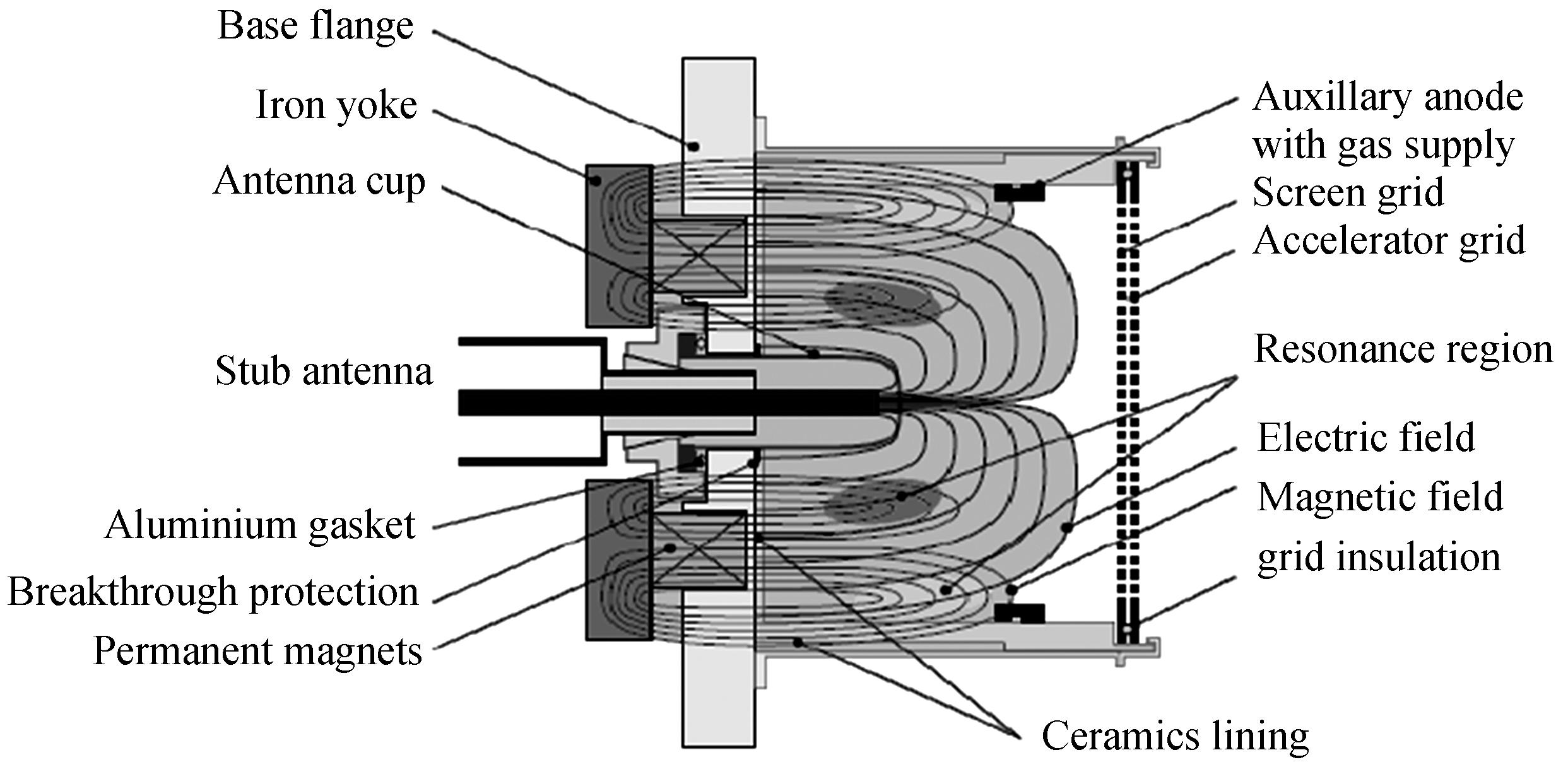
    Fig. 1. Schematic diagram of the working principle of the microwave cyclotron resonance ion source
    Ridge structure impurity target
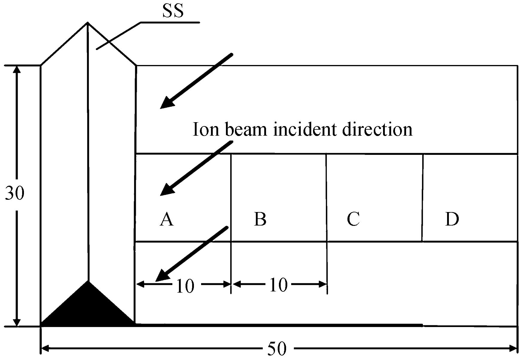
    Fig. 2. Ridge structure impurity target
    AFM topography and Fourier transform of sapphire sputtered by Ar+ ion beam with or without impurities
    Fig. 3. AFM topography and Fourier transform of sapphire sputtered by Ar+ ion beam with or without impurities
    PSD curve graph of Ar+ ion beam sputtering sapphire surface with or without impurity assistance(Ubeam=1000 eV,
    Fig. 4. PSD curve graph of Ar+ ion beam sputtering sapphire surface with or without impurity assistance(Ubeam=1000 eV,
    Schematic diagram of island structure formation process
    Fig. 5. Schematic diagram of island structure formation process
    AFM image and Fourier transform of the sapphire sample surface after etching with different incident energ(αion=65°,Jion=487 μA/cm2,T=60 min)
    Fig. 6. AFM image and Fourier transform of the sapphire sample surface after etching with different incident energ(αion=65°,Jion=487 μA/cm2,T=60 min)
    PSD curves and trends of height and RMS of nanostructures on the surface of sapphire samples after etching with different incident energy (αion=65°,Jion=487 μA/cm2,T=60 min)
    Fig. 7. PSD curves and trends of height and RMS of nanostructures on the surface of sapphire samples after etching with different incident energy (αion=65°,Jion=487 μA/cm2,T=60 min)
    Surface topography of sapphire sample etched with 1200 eV energy
    Fig. 8. Surface topography of sapphire sample etched with 1200 eV energy
    Ion beam parametersParameter setting
    Background vacuum2×10-3 Pa
    Working vacuum2.5×10-2 Pa
    Accelerating voltage(Uacc350 eV
    Ion beam incident angle(αion65°
    Beam current density(Jion487 μA/cm2
    Etching time(T60 min
    Table 1. Process experiment parameters
    Li TANG, Zhili CHEN, Yuzhao LIU, Qian BI, Yingxue XI, Weiguo LIU. Metal-assisted Low-energy Ar+ Ion Beam Induces Self-organized Nanostructure of Sapphire[J]. Acta Photonica Sinica, 2021, 50(2): 183
    Download Citation