1State Key Laboratory of Advanced Optical Communication Systems and Networks, School of Electronics Engineering and Computer Science, Peking University, Beijing 100871, China
2Frontiers Science Center for Nano-optoelectronics, Peking University, Beijing 100871, China
3State Key Laboratory on Integrated Optoelectronics, Institute of Semiconductors, Chinese Academy of Sciences, Beijing 100083, China
We demonstrate a package-level passive equalization technology in which the wire-bonding-induced resonance effect is used to compensate for the limited gain strength within the Nyquist frequency. The corresponding gain strength under various inductance and capacitance combinations could be quantitatively determined using a numerical simulation. With the increase in the Nyquist frequency, the capacitance shows a greater effect on the gain strength than the inductance. Therefore, the parasitic capacitance should be decreased to realize the desired gain strength at a higher Nyquist frequency. With this equalization technology, gain strength of 5.8 dB is obtained at 22 GHz, which can compensate for the limited bandwidth for the 112 Gbps pulse amplitude modulation (PAM4) signal. The experimental results show that 112 Gbps/ PAM4 transmission based on a directly modulated laser (DML) module can be realized with a bit error rate of 1 × 10 3 at a received optical power of 3 dBm.
With the rapid development of high technology, such as artificial intelligence, virtual reality, driverless vehicles, and 5G communication, data traffic has increased at a rate of 30% year to year[1,2]. To solve the capacity bottleneck, data centers have been developed toward higher transmission speeds. Therefore, beyond 100 Gbps per lane optical transmission systems have attracted research interest and have been considered the best solution, owing to their simplicity and cost-effectiveness[3–6]. Recently, the 100G Lambda Multi-Source Agreement (MSA) Group released 100G-FR (∼2 km), 100G-LR (10 km), and 400G-FR4 (10 km) technical specifications (Rev 2.0), which depend on the 100 Gbps per lane optical technology along with the four-level pulse amplitude modulation (PAM4) format[7]. Furthermore, a directly modulated laser (DML) operating at the O band (1310 nm) has been considered a promising candidate owing to advantages such as low cost, high linearity, and negligible dispersion[8]. However, compared with the external modulation scheme, the DML has an inferior bandwidth, resulting in a severe transmission loss in the high-frequency range. The loss of high-frequency signal can cause inter-symbol interferences (ISIs), which deteriorate the transmission performance. For a 112 Gbps PAM4 signal, the corresponding Nyquist frequency is approximately 28 GHz. Therefore, equalization techniques are commonly employed to make up for the limited bandwidth of the DML and strengthen the transmission link response within the Nyquist frequency, such as the decision feedback equalizer (DFE), feed-forward equalizer (FFE), and continuous time linear equalizer (CTLE)[9–11].
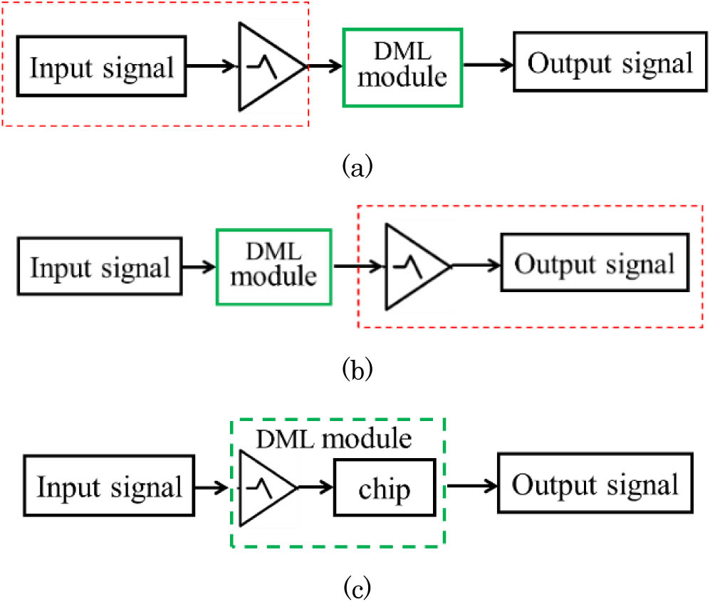
Passive equalization techniques have been widely used in high-speed signal transmission, effectively preventing bandwidth degradation in the high-frequency range and improving the high-frequency characteristics of the transmission link[12–14]. In addition, compared with an active equalizer, a passive equalizer has lower power consumption, smaller size, lower circuitry costs, and can be easily realized. Currently, transmitter (TX) equalization and receiver (RX) equalization are two common types of equalization processes, as shown in Figs. 1(a) and 1(b), respectively. The former is also called pre-equalization. The two equalization techniques can be used to compensate for the limited bandwidth of the DML and have largely the same effect on the improvement in the transmission signal quality. However, the design procedure of the two equalization circuits is rather complicated: the values of the passive components, such as the resistor and capacitor, need to be accurately adjusted, and the designed circuit should be then translated into a complementary metal–oxide–semiconductor (CMOS) chip or a microstrip line circuit with the equalization function.
In this Letter, we report a simple and low-cost package-level passive equalization technique, as shown in Fig. 1(c). The DML module comprises a package network and an intrinsic chip. Conventionally, a package network has a flat response in the low-frequency range after undergoing a rapid drop in the high-frequency range, thus exhibiting a low-pass filtering characteristic. This results in a maximum bandwidth degradation of 3 dB in the intrinsic DML chip. Therefore, the transmission curve characteristic of the packaged DML module cannot meet the demand of a 112 Gbps PAM4 modulation signal. For the package network, a wire bonding process is necessary to connect the different pads. This inevitably introduces parasitics, which are generally unwanted because of their bandwidth suppression. Nevertheless, parasitics can lead to a resonance effect when the inductance and capacitance are suitable[15–17]. Therefore, a properly designed package network can exhibit a high-pass filtering characteristic, which helps in improving the high-frequency response of the transmission channel. In this study, we confirm that the proposed passive equalization technique can enable 112 Gbps per lane PAM4 signal transmission.
Sign up for Chinese Optics Letters TOC. Get the latest issue of Chinese Optics Letters delivered right to you!Sign up now
To demonstrate the influence of the equalization on the frequency response within the DML module, a simplified equivalent circuit is developed. The transmission response of the high-frequency package network, shown in Fig. 2, can be expressed as follows: where the subscripts P, A, and E represent the package network, the package assembly, and the passive equalization network, respectively. The package assembly mainly comprises a high-frequency conical connector and a transmission line. Its frequency response can be measured and exported as an s2p file using a vector network analyzer. It can then be embedded using a T-parameter matrix, which is expressed as follows: where the subscripts 1 and 2 refer to the ports of the package assembly. As the package assembly only comprises passive components, the S-parameter matrix is a reciprocal network. Thus, we have .
Figure 2.Circuit model for the high-frequency package network of a DML. The S parameters of the package assembly are measured using the vector network analyzer, and the s2p file is embedded in the circuit. The inset shows the bond wire between the chip pad and the package assembly.
A bond wire is commonly used to realize the electrical connection between the transmission line and the chip pad. In the high-frequency range, the bond wire exhibits a strong inductance characteristic and can be treated as a low-pass filter. Thus, the high-frequency transmission response exhibits a rapid drop and limits the bandwidth of the DML module. The inductance value is mainly determined by the length of the bond wire. When the bond wire is welded on the surface of the chip pad, a parasitic capacitance is inevitably introduced. With proper parameter values of the inductance and capacitance, a resonance effect can be stimulated at some frequency points; thus, the transmission response of the package network can have a high-pass filtering characteristic, making the network a passive equalizer. The resonance effect is comprehensively studied using a resistor–inductor–capacitor (RLC) circuit, as shown in Fig. 2. The transmission response of the passive equalization network can be expressed as follows: where and represent the wire-bonding-induced inductance and capacitance, respectively, and denotes the input equivalent impedance. We simulate the equalization performance with respect to the frequency under various inductance and capacitance combinations, wherein the inductance value is varied from 0 to 1 nH with a 0.1 nH step, and the capacitance is varied from 0 to 0.1 pF with 100 fF steps. Figure 3 shows the simulated gain strength at six frequency points. With the increase in the frequency, the upper limit of the gain strength extends from ∼3 to ∼10 dB. Furthermore, compared with the inductance, the capacitance plays a more dominant role on the equivalent performance at all the frequency points, and the effective weight is enhanced with the increase in the frequency. At a frequency of 35 GHz, it is impossible to achieve a gain characteristic if the capacitance value exceeds approximately 90 fF. This shows that the parasitic capacitance should be decreased as much as possible for proper gain strength. In a practical process, the capacitance value is closely related to the bonding pad area. A smaller bonding pad area has a strong impact on the degradation of the capacitance value. Generally, there are two methods of miniaturizing the bonding pad. One of the methods involves reducing the diameter of the bond wire, such as from 25 to 18 μm. However, a smaller bond wire diameter will cause a more serious inductance effect, limiting further improvement in the cut-off frequency. The other method is to use wedge bonding. Compared with wire ball bonding, in which a ball with a diameter approximately 2.5 times the wire diameter is formed at the end of the wire, wedge bonding leads to a smaller bonding pad area and a lower parasitic capacitance. Thus, we selected wedge bonding as the wire bonding process.
Figure 3.Contour maps of gain strength versus inductance and capacitance at frequencies of 10, 15, 20, 25, 30, and 35 GHz.
To determine the bonding-induced capacitance value when using wedge bonding, we designed a measure fixture in which two independent coplanar waveguide (CPW) transmission lines are connected by a bond wire, as shown in the inset of Fig. 4. The influence of the CPW transmission lines can be measured using a high-frequency microwave probe and deducted using the de-embed operation in the advanced design system (ADS) software. In a previous report[17], the inductance was found to be approximately 1 nH/mm for a 25 μm diameter bond wire. Here, the bond wire length was 0.58 mm, and thus, the inductance was 0.58 nH. An equivalent circuit was built to extract the capacitance. Figure 4 shows that the simulation result is in good agreement with the measurement result, and the capacitance value is estimated to be 57.8 fF. For a mature wedge bonding process and for a defined wire bonding substrate, the capacitance can be considered a constant. Therefore, it is feasible to realize the desired gain strength only by adjusting the length of the bond wire.
Figure 4.Measured (symbol lines) and simulated (solid lines) transmission parameters of the bond wire used in the DML module. The inset shows the designed measure fixture and the equivalent circuit model used to extract the bonding-induced capacitance.
Based on the above theoretical analysis, we built two measure schemes with and without equalization. In the equalization scheme, two types of bond wires are prepared for the DML package: type 1 with an optimal bond wire length of 0.6 mm and type 2 with a bond wire length of 0.35 mm. Both of the bond wires have a diameter of 25 μm and are wedge-bonded on the metallic pads. Figure 5 shows the gain strength under the proposed conditions at 22 GHz. The gain values are approximately 5.8 and 2.8 dB, respectively.
Figure 5.Contour map of gain strength versus inductance and capacitance at 22 GHz. The labels show the corresponding gain strengths under the two bond wire length conditions.
Figure 6 shows the measured transmission responses of the DML module under different conditions. A significant difference is observed between the three transmission curve characteristics, although the bandwidth reaches near 27 GHz. Without equalization, the curve is degraded linearly. However, with equalization, boost gains of 6 and 3 dB are obtained at 22 GHz for the type 1 and 2 cases, respectively. This shows that the experimental results are in good agreement with the analytical results.
Figure 6.Frequency responses of the DML module packaged with and without equalization conditions, measured at a laser current of 90 mA.
To evaluate the effect of different equivalent gain strengths on the modulation performance of the DML, an experimental setup for single-wavelength PAM4 signal transmission is built, as shown in Fig. 7. On the TX side, an arbitrary waveform generator (AWG) operated at 92 GSa/s with an analog bandwidth of 32 GHz was used to generate a pseudo-random binary sequence (PRBS) , PAM4 signal. To compensate for the electrical channel loss, a pre-emphasis was implemented in the AWG using its calibration software. The generated signal was directly injected into the proposed DML. As shown in Fig. 7, the eye diagram of the 112 Gbps PAM4 signal from the AWG is clearly opened. Owing to the improved high-frequency microwave circuit[18], the signal injection efficiency is enhanced. Therefore, a drive voltage as low as 1 V is sufficient, indicating that the DML can be directly driven using a serializer/deserializer (SerDes). This will be cost-effective, as an electrical amplifier is not required. The modulated optical signal is launched into the standard single-mode fiber (SSMF) with a transmission loss of 0.35 dB/km at the O band. The optical signal is then received and converted to an electrical signal using positive-intrinsic-negative (PIN)-type photodiodes integrated with a transimpedance amplifier (TIA), with a bandwidth of 32 GHz. To control the received optical power (ROP), a variable optical attenuator (VOA) was used. Finally, the electrical signal was sampled using a real-time digital sampling oscilloscope operated at 80 GSa/s and processed off-line to calculate the bit error rate (BER).
Figure 7.Experimental setup for single-wavelength PAM4 signal transmission.
Figure 8 shows the measured BER performance under various modulation speed conditions. The BER performance result is quite different. When the modulation speed is 56 Gbps, the BER is largely the same (approximately ). This is because the Nyquist frequency of the 56 Gbps signal is only 14 GHz. The bandwidth of the DML for the three cases is high enough. Therefore, at a Nyquist frequency of 14 GHz, the DML exhibits only slight bandwidth degradation. However, with the increase in the modulation speed, the BER performance without equalization deteriorates rapidly and only reaches up to 90 Gbps at the forward error correction (FEC) limit. With equalization, for the type 2 case, when the modulation speed increases to 100 Gbps, the BER reaches the FEC limit (). By this time, the BER for the type 1 case is reduced by one order of magnitude and is only . At a modulation speed of 112 Gbps, only the BER for the type 1 case is lower than the FEC limit. This shows that the 5.8 dB boost gain introduced using the proposed method at a Nyquist frequency of 22 GHz brings an excellent equivalent performance and effectively improves the high-frequency response under the 112 Gbps PAM4 modulation condition.
Figure 8.BER versus the modulation speed with and without equalization cases.
We further studied the received sensitivity of the 56 Gbaud PAM4 signal for the back-to-back (BtB) case, as shown in Fig. 9. With the increase in the ROP, the BER decreases and reaches the FEC limit at an ROP of approximately . However, when the ROP exceeds 3 dBm, the BER performance is deteriorated. It may reach up to the saturated input power of the photodiodes used. Finally, an optimal BER of is obtained.
Figure 9.BER of 112 Gbps PAM4 signal versus the ROP for the BtB case.
From these results, we can conclude that the previously developed DML module can be used for 112 Gbps PAM4 operation in an ultra 100G per wavelength optical communication system. Furthermore, four or more DMLs can be integrated into a module to realize , , and even systems. This will significantly enhance the communication capacity of data centers.
In summary, a package-level passive equalization technology is proposed for realizing 112 Gbps/ PAM4 transmission. The effect of wire-bonding-induced parasitics on the equalization gain strength was quantitatively investigated. The detailed analysis and simulation results showed that with the increase in the Nyquist frequency, the parasitic capacitance has a more significant effect on the gain strength than the parasitic inductance. To realize the desired gain strength at a high frequency, the parasitic capacitance should be decreased. Furthermore, the wire-bonding-induced parasitic capacitance was determined by fitting with the measurement result. Thus, various gain strengths could be realized by adjusting only the length of the bond wire. With the proposed equalization scheme, a 112 Gbps PAM4 transmission experiment based on the DML module was carried out with two types of gain strengths at 22 GHz. The BER was lower than the FEC limit only in the case of type 1 (optimal bond wire length: 0.58 mm). The optimal BER could reach up to for an ROP of 3 dBm. The measurement results confirmed that the proposed equalization technology can effectively compensate for the gain loss within the Nyquist frequency and can be considered a solution to limited device bandwidth for ultra 100G per lane optical communication technology.
[3] C. Yang, R. Hu, M. Luo, Q. Yang, C. Li, H. Li, S. Yu. IEEE Photon. J., 8, 7903907(2016).
[4] Y. Gao, J. C. Cartledge, S. S.-H. Yam, A. Rezania, Y. Matsui. Proceedings of VDE, 42nd European Conference on Optical Communication, 1(2016).
[5] W. Wang, P. Zhao, Z. Zhang, H. Li, D. Zang, N. Zhu, Y. Lu. Optical Fiber Communication Conference, Th4B-8(2018).
[6] J. Zhang, J. Yu, X. Li, Y. Wei, K. Wang, L. Zhao, W. Zhou, J. Xiao, X. Pan, B. Liu, X. Xin, L. Zhang, Y. Zhang. Optical Fiber Communication Conference (OFC), Tu2F.1(2019).