
Meng Deng, Zichun Liao, Yankai Chen, Ningning Yang, Xu Yan, Chi Zhang, Nengli Dai, Yi Wang. On-chip ultrafast pulse generation based on graphene-silicon hybrid waveguides[J]. Photonics Research, 2021, 9(9): 1660
- Photonics Research
- Vol. 9, Issue 9, 1660 (2021)
Abstract
1. INTRODUCTION
Ultrafast pulse lasers have a plethora of applications ranging from automatic driving and terahertz generation to biological detection and optical metrology [1,2]. The successful tabletop Ti:sapphire pulse lasers are capable of delivering tens of femtosecond pulse width and pico-joule pulse energy, which are the basic instruments for nonlinear optics in free space [3]. Fiber pulse lasers, holding the light at the core of fiber, exhibit hundreds of femtoseconds pulse width and lower pulse energy [4]. As the ultrafast pulse lasers are key elements for nonlinear photonics, Ti:sapphire or fiber pulse lasers have been used to characterize the fruitful nonlinear processes within integrated optical waveguides, such as silicon, III-V, and chalcogenide related. There is great demand for integrated pulse lasers on the silicon photonics platform because of the advanced advantages resulting from the shrinkage of footprint, reduction of power consumption, and solidarity of device stability. Silicon waveguides also suffer intrinsic strong two-photon absorption under pumping light and slow recombination of subsequent free carriers, leading to nanosecond recombination time and tens of picoseconds mode-locking pulse [5,6]. Although the III-V on silicon pulse laser has been realized, pulse width with typically a few picoseconds duration is still limited by the transient process of free carriers in III-V material [7].
Since first deposited by mechanical exfoliation in 2004 [8], graphene has attracted strong interest in optoelectronics. Graphene is regarded as an excellent broadband saturable absorber (SA) for its ultrafast recovery time [9] and high damage threshold. In recent years, graphene has been widely introduced into optoelectronic platforms for modulators, detectors, and polarizers [10–14]. Patterned graphene on a waveguide does not change the original optical mode. Moreover, the interaction between graphene and the evanescent wave of a waveguide not only elongates the optical interaction length [15] but also enhances the performance of the device [16].
Here, we demonstrate an ultrafast laser based on a graphene/silicon hybrid waveguide (GSHW), which has recently attracted considerable attention as a promising host of free carrier manipulation at the atomic scale [17]. Besides, graphene resting on the silicon waveguide, patterned with standard photolithography process, provides strong light–matter interaction (), which is almost two orders of magnitude greater than that of the counterpart of graphene on fiber [18]. The pump–probe experiment shows that the GSHW has an ultrafast carrier recovery time of 1.82 ps, which is a cornerstone for the formation of ultrafast pulses. The several 10 μm saturable absorption region working with the evanescent coupling scheme improves the modulation effect of SA while reducing the saturable pulse energy within chip-scale, resulting in the mode-locking self-starting phenomenon, which can still be observed under the condition of large intracavity loss (). Finally, the duration of laser output pulse is measured to be 542 fs, with a fundamental repetition rate of 54.37 MHz. Taking the mode area of the waveguide into account, the peak power density on-chip exceeds , which provides convenience for all-optical signal processing and nonlinear optical applications on chip.
Sign up for Photonics Research TOC. Get the latest issue of Photonics Research delivered right to you!Sign up now
2. SAMPLE PREPARATION AND CHARACTERIZATIONS
Figure 1(a) shows the structure of the GSHW: the silicon waveguide with a ridge height of 200 nm and ridge width of 500 nm is fabricated on a silicon on insulator (SOI) wafer with a 340 nm top silicon layer. Both ends of the waveguides are connected by strip gratings with an etching depth of 200 nm. The period and duty cycle of coupling grating are 600 nm and 0.45, respectively. The grating is optimized for TE polarization mode; the coupling loss is measured to be 7 dB per facet. The waveguides and gratings are exposed by electron-beam lithography (Vistec EBPG 5000plus ES) and then etched by inductively coupled plasma (Oxford Plasmalab system 100 ICP 180). Then, the monolayer graphene grown on the copper foil by chemical vapor deposition is transferred onto the silicon waveguide via wet transfer method [19]. After the transfer process, the graphene layer is then patterned by UV exposure and etched by the reactive ion etching process. Finally, a certain length of graphene remains on the silicon waveguide to form the GSHW. The optical waveguide mode couples to the graphene layer through the evanescent wave, as shown in Fig. 1(b). Although the modal confinement factor [20] of the graphene layer is almost neglectable (), remarkable propagation losses could still be achieved by the accumulated evanescent interaction between graphene pads and the silicon ridge waveguides over several tens of micrometers. Propagation losses of the GSHWs were characterized by the cutback method [21], which indicates an absorption coefficient of . This is close to the simulation result of , for which we attribute the simulation error to the neglect of graphene on both sides of the waveguide.
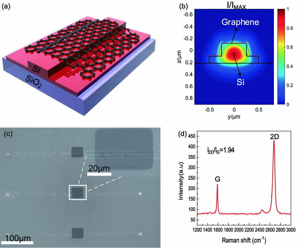
Figure 1.Hybrid graphene/silicon waveguide device. (a) Diagram of the GSHW. (b) Quasi-TE mode distribution of GSHW. It can be seen from (a) and (b) that graphene is located in the optical field region of the silicon waveguide and interacts with the evanescent wave. (c) SEM image of prepared GSHWs. Inset shows the patterned graphene on silicon waveguide. (d) Raman spectrum of monolayer graphene on silicon waveguide.
Figure 1(c) shows the scanning electron microscope (SEM) image of fabricated GSHWs. Each GSHW contains a 60 μm long monolayer graphene. The figure inset shows the detailed graphene pad patterned on the ridge waveguide, from which the patterned graphene rests on the silicon waveguide. The samples are analyzed with a Raman microscopy system (LabRAM HR800) using a 532 nm wavelength laser [Fig. 1(d)]. Raman spectrum of the GSHW shows that the graphene pads are with single layer and high crystallinity. The G peak of graphene is located at , the 2D peak is at , and the is calculated to be 1.94. Therefore, it turns out that graphene is monolayer [22,23]. The state of low defects keeps the carrier mobility of graphene at a high level, ensuring the ultrafast carrier response time of the atomic-thin graphene/silicon junction.
3. EXPERIMENT SETUP AND RESULTS
A. SA of GSHW
![]()
Figure 2.Saturable absorption property of the GSHW. (a) Schematic of GSHW saturation absorption experiment setup. VOA represents the variable optical attenuator; PM is the power meter. (b) The transmittance as a function of the average optical power. The average power is the remaining input power by exclusion of the insertion loss of single-ended grating coupler. Experimental data are represented by black dots. The red solid line corresponds to a fit with a two-level saturable absorber model.
As can be seen from Table 1, because of the strong coupling effect between the graphene pad and waveguide evanescent wave, the modulation depth of our GSHW is relatively higher than in previous results. Our GSHW only needs tens of micrometers of graphene to achieve a better modulation effect than the millimeter-scale graphene of fiber lasers. Benefiting from the ultrasmall mode area of the silicon waveguide, our GSHW needs low pulse energy to reach saturation, which is two orders of magnitude lower than the previous results. Futhermore, the evanescent coupling way of GSHW increases the damage threshold of graphene compared with the traditional sandwich structure.
B. Mode-Locked Laser Setup Based on GSHW
Figure 3 shows the experimental setup of the hybrid graphene/silicon ultrafast laser. The commercial erbium-doped fiber [LIEKKI Er110-4/125, group velocity dispersion (GVD), ] with high doping concentration is used as the gain medium in the cavity. The cavity was optically pumped by a 980 nm laser diode (980 LD); the maximum pump power of 980 LD is 900 mW. A 980/1550 WDM, a polarization-independent isolator, and a polarization controller are connected by single-mode fiber (SMF-28; GVD, ) in order in the cavity. Our GSHW is embedded in the laser cavity system as a saturable absorber. The 90/10 fiber optical coupler is inserted into the ring cavity for laser output. Taking the coupling loss of the grating, the absorption loss of the hybrid waveguide, and the insertion loss of other devices into account, the total loss in the cavity is about 20 dB. The total cavity length of the laser system is 3.77 m, which contains a 0.8 m erbium-doped fiber, 0.15 m pigtails of WDM (OFS 980; GVD, ), and 2.82 m single-mode fiber. The dispersion of GSHW () can be ignored due to its short length. The total dispersion of the system is calculated to be . An oscilloscope, a spectrometer, and an autocorrelator are connected to the output port of the laser, respectively.
![]()
Figure 3.Schematic of mode-locked laser setup based on GSHW, where the GSHW acts as saturable absorber.
Although the cavity loss is large, the laser still achieves a self-starting passive mode-locking operation at the pump power of 200 mW. The reason for this phenomenon is that GSHW only needs low pulse energy to reach saturation. Figure 4(a) shows the optical spectrum of the laser output, the 3 dB bandwidth is measured to be 3.57 nm at a central wavelength of 1546 nm. At mode-locked state, the pulse train measured at the output port is shown in Fig. 4(b). Figure 4(b) shows that the pulse trains have a pulse interval of 18.3 ns, which matches the cavity roundtrip time for the total cavity length. The pulse duration is measured by a commercial autocorrelator (Pulsecheck, APE). Due to the large coupling loss of the grating, the maximum output power of the laser cavity at mode-locked state is 0.5 mW, which is lower than the power response range of the autocorrelator, so an EDFA is connected to the output end to characterize the pulse duration. The measured intensity autocorrelation (AC) trace is shown in Fig. 4(c). Fitting the autocorrelation trace with a hyperbolic-secant profile and multiplying the AC trace width with a decorrelation factor, the actual duration of the measured pulse is 542 fs. We also measured the RF spectrum of the mode-locked pulses with a span of 200 MHz and a resolution of 100 Hz. As shown in Fig. 4(d), the fundamental repetition rate is 54.37 MHz. The insert shows that the background noise level of the spectrum is 47 dB, which means the mode-locking operation works at a stable state. Once the mode-locking state is achieved, there is no need to use external feedback. Mode-locking operation maintains stable for almost 1 h during the experiment. In addition, we introduce a silicon waveguide with the same structural parameters as GSHW into the same laser cavity. Even if the pump power is increased to the maximum output value of 980 LD (900 mW), the mode-locked state does not occur. This also confirms that our GSHW plays a fundamental role in pulse narrowing.
![]()
Figure 4.Characteristics of passively mode-locked operation. (a) Laser output optical spectrum with 3 dB bandwidth of 3.57 nm. (b) Pulse train of fundamental mode-locked operation. Insert shows a pulse interval of 18.3 ns. (c) Autocorrelation trace of mode-locked operation. The experimental data are represented by black lines. Red curve represents fitting using a hyperbolic-secant function. The FWHM of the autocorrelation trace is 836 fs, corresponding to a pulse duration of 542 fs (a deconvolution factor of 0.648 is used to account for the hyperbolic-secant pulse shape). (d) The RF spectrum of the mode-locked pulses, corresponding to the repetition frequency of 54.37 MHz. Insert shows that the SNR is equal to 47 dB.
C. Pump-Probe Experiment
Regarding the formation mechanism of the ultrafast pulse in the laser cavity, it can be attributed to the ultrafast carrier response of graphene/silicon junction in GSHW. To confirm this, we quote a pump–probe experiment system, as shown in Fig. 5(a). The system consists of two NPR pulsed light sources with a central wavelength around 1560 nm. The duration of the two pulses is about 700 fs; the bandwidth is about 15 nm. In our system, the repetition rates of the pump light (Pulse 1) and probe light (Pulse 2) are 92.868 and 92.867 MHz, respectively. The repetition rate difference between the two pulses is 1 kHz, which results in a time scaling up factor of 92,800. Pulse 1 is filtered by a bandpass optical filter to produce pump light with a central wavelength of 1555 nm and a bandwidth of 8 nm. The pump light enters the GSHW through Port 1 of the optical circulator. The probe light enters GSHW through ISO, VOA, and PC and then transmits by the optical circulator from Port 2 to Port 3. There is also a bandpass filter connected to the detection part that only allows light with wavelength larger than 1560 nm, thus avoiding the detection of pump light reflected by the grating coupler. Polarization controllers (PCs) are adopted to achieve optimized coupling efficiency. The VOA is used to control the intensity of the pump and probe light. The blue line in Fig. 5(b) shows the spectrally integrated transmission change of the probe light as a function of the pump–probe delay (, : the transmission of GSHW with and without pump excitation). Our experimental data are obtained by using the high-speed asynchronous sampling method [30–32]. The falling edge of the curve indicates that the free-carrier recombination time of the GSHW is as short as 1.82 ps, which is three orders of magnitude faster than that of the silicon waveguide [33–35]. Illustration ① in Fig. 5(b) represents the recombination state of photogenerated carriers in GSHW. Compared with that of silicon waveguides, as shown in Illustration ②, the carrier recombination in GSHW occurs at the interface between graphene and Si, while the recombination of Si waveguides occurs inside bulk Si, which results in a larger carrier recombination area and slower recombination rate. The recombination process occurs at the graphene/silicon interface ensures the ultrafast carrier response time and facilitates pulse narrowing. Besides, there is negative “tails” of kinetics shown in Fig. 5(b). Previous literature attributed that negative region to the thermal diffusion and shrinkage of band separation caused by lattice heating [36,37]. The carrier exchange between substrate (Si) and graphene also leads to similar experimental phenomena [38,39].
![]()
Figure 5.Ultrafast carrier response of graphene/silicon junction. (a) Schematic of the carrier response measurement setup with a pump–probe system. (b) The carrier response of GSHW under pump light. The blue solid line is the experimental measurement result. The falling edge of the experimental curve shows that the carrier relaxation recombination time of the graphene/silicon junction is as short as 1.82 ps. Illustration ① represents the carrier recombination state shown on the falling edge of the curve. Illustration ② shows the recombination state of photogenerated carriers in a pure silicon waveguide.
4. CONCLUSION
In summary, we have experimentally demonstrated an ultrafast laser based on a GSHW. When the incident light enters GSHW, a large number of photogenerated carriers are generated. Then, the photogenerated carriers tend to recombine at the silicon–graphene interface rather than in silicon. The recombination time of the carrier near the graphene/silicon junction is as short as 1.82 ps, which is three orders of magnitude faster that of than silicon. Our result is different from the previous conclusions of Cheng
Compared with the silicon waveguides, the carrier response rate of GSHW is increased by nearly three orders of magnitude. The ultrafast carrier response of the GSHW is conducive to pulse narrowing. Based on the fact that GSHW can reach saturation at low pulse energy, although the intracavity loss is higher than 20 dB, the laser cavity can still achieve a self-start mode-locking state. The pulse width is measured to be 542 fs with a repetition rate of 54.37 MHz. Mode-locking operation maintains stability for hours during experiments. The power density on the hybrid waveguide in the mode-locked state exceeds , which is sufficient to excite various nonlinear effects of the silicon waveguide [42–44]. This is a favorable result for the application of on-chip supercontinuum sources and other nonlinear effects. Our work, along with previous results, provides broad application prospects for nonlinear optics and a feasible solution for silicon-based integrated pulsed light sources.
Acknowledgment
Acknowledgment. We thank all engineers in the Center of Micro-Fabrication and Characterization (CMFC) of Wuhan National Laboratory for Optoelectronics (WNLO) for the support in fabrication. We thank Guo-Qin Liu for early exploration in process and fabrication.
References
[1] F. Dausinger, F. Lichtner. Femtosecond Technology for Technical and Medical Applications, 96(2004).
[2] U. Keller. Recent developments in compact ultrafast lasers. Nature, 424, 831-838(2003).
[3] F. Canbaz, N. Kakenov, C. Kocabas, U. Demrbas, A. Sennaroglu. Generation of sub-20-fs pulses from a graphene mode-locked laser. Opt. Express, 25, 2834-2839(2017).
[4] Q. Bao, H. Zhang, Y. Wang, Z. Ni, Y. Yan, Z. X. Shen, K. P. Loh, D. Y. Tang. Atomic-layer graphene as a saturable absorber for ultrafast pulsed lasers. Adv. Funct. Mater., 19, 3077-3083(2009).
[5] E.-K. Tien, N. S. Yuksek, F. Qian, O. Boyraz. Effect of TPA and FCA interplay on pulse compression in silicon. LEOS IEEE Lasers and Electro-Optics Society Annual Meeting Conference, 888-889(2007).
[6] E.-K. Tien, N. S. Yuksek, F. Qian, O. Boyraz. Pulse compression and modelocking by using TPA in silicon waveguides. Opt. Express, 15, 6500-6506(2007).
[7] B. R. Koch, A. W. Fang, O. Cohen, J. E. Bowers. Mode-locked silicon evanescent lasers. Opt. Express, 15, 11225-11233(2007).
[8] K. S. Novoselov, A. K. Geim, S. V. Morozov, D. Jiang, Y. Zhang, S. V. Dubonos, I. V. Grigorieva, A. A. Firsov. Electric field effect in atomically thin carbon films. Science, 306, 666-669(2004).
[9] M. Breusing, S. Kuehn, T. Winzer, E. Malić, F. Milde, N. Severin, J. Rabe, C. Ropers, A. Knorr, T. Elsaesser. Ultrafast nonequilibrium carrier dynamics in a single graphene layer. Phys. Rev. B, 83, 153410(2011).
[10] S. Marconi, M. Giambra, A. Montanaro, V. Mišeikis, S. Soresi, S. Tirelli, P. Galli, F. Buchali, W. Templ, C. Coletti, V. Sorianello, M. Romagnoli. Photo thermal effect graphene detector featuring 105 Gbit s−1 NRZ and 120 Gbit s−1 PAM4 direct detection. Nat. Commun., 12, 806(2021).
[11] D. Mao, C. Cheng, F. Wang, Y. Xiao, T. Li, L. Chang, A. Soman, T. Kananen, X. Zhang, M. Krainak, P. Dong, T. Gu. Device architectures for low voltage and ultrafast graphene integrated phase modulators. IEEE J. Sel. Top. Quantum Electron., 27, 3400309(2020).
[12] B. Jiang, Y. Hou, H. Wang, X. Gan, A. Li, Z. Hao, K. Zhou, L. Zhang, J. Zhao. Few-layer graphene integrated thin tilted fiber grating for all-optical switching. J. Lightwave Technol., 39, 1477-1482(2020).
[13] M. A. Giambra, V. Mišeikis, S. Pezzini, S. Marconi, A. Montanaro, F. Fabbri, V. Sorianello, A. C. Ferrari, C. Coletti, M. Romagnoli. Wafer-scale integration of graphene-based photonic devices. ACS Nano, 15, 3171-3187(2021).
[14] C. Zhong, J. Li, H. Lin. Graphene-based all-optical modulators. Front. Optoelectron., 13, 114-128(2020).
[15] Y. Su, Y. Zhang, C. Qiu, X. Guo, L. Sun. Silicon photonic platform for passive waveguide devices: materials, fabrication, and applications. Adv. Mater. Technol., 5, 1901153(2020).
[16] Y. Yao, Z. Cheng, J. Dong, X. Zhang. Performance of integrated optical switches based on 2D materials and beyond. Front. Optoelectron., 13, 129-138(2020).
[17] A. Di Bartolomeo. Graphene Schottky diodes: an experimental review of the rectifying graphene/semiconductor heterojunction. Phys. Rep., 606, 1-58(2016).
[18] J. Zapata, D. Steinberg, L. A. Saito, R. De Oliveira, A. Cárdenas, E. T. De Souza. Efficient graphene saturable absorbers on D-shaped optical fiber for ultrashort pulse generation. Sci. Rep., 6, 20644(2016).
[19] V. Sorianello, M. Midrio, G. Contestabile, I. Asselberghs, J. Van Campenhout, C. Huyghebaert, I. Goykhman, A. Ott, A. Ferrari, M. Romagnoli. Graphene–silicon phase modulators with gigahertz bandwidth. Nat. Photonics, 12, 40-44(2018).
[20] Z. Ma, M. H. Tahersima, S. Khan, V. J. Sorger. Two-dimensional material-based mode confinement engineering in electro-optic modulators. IEEE J. Sel. Top. Quantum Electron., 23, 81-88(2016).
[21] R. Kou, S. Tanabe, T. Tsuchizawa, K. Warabi, S. Suzuki, H. Hibino, H. Nakajima, K. Yamada. Characterization of optical absorption and polarization dependence of single-layer graphene integrated on a silicon wire waveguide. Jpn. J. Appl. Phys., 52, 060203(2013).
[22] A. C. Ferrari, J. C. Meyer, V. Scardaci, C. Casiraghi, M. Lazzeri, F. Mauri, S. Piscanec, D. Jiang, K. S. Novoselov, S. Roth. Raman spectrum of graphene and graphene layers.. Phys. Rev. Lett., 97, 187401(2006).
[23] M. Bayle, N. Reckinger, J. R. Huntzinger, A. Felten, A. Bakaraki, P. Landois, J. F. Colomer, L. Henrard, A. A. Zahab, J. L. Sauvajol. Dependence of the Raman spectrum characteristics on the number of layers and stacking orientation in few-layer graphene. Phys. Status Solidi, 252, 2375-2379(2015).
[24] P. Demongodin, H. El Dirani, J. Lhuillier, R. Crochemore, M. Kemiche, T. Wood, S. Callard, P. Rojo-Romeo, C. Sciancalepore, C. Grillet, C. Monat. Ultrafast saturable absorption dynamics in hybrid graphene/Si3N4 waveguides. APL Photon., 4, 076102(2019).
[25] E. Garmire. Resonant optical nonlinearities in semiconductors. IEEE J. Sel. Top. Quantum Electron., 6, 1094-1110(2000).
[26] H. Wang, N. Yang, L. Chang, C. Zhou, S. Li, M. Deng, Z. Li, Q. Liu, C. Zhang, Z. Li, W. Yi. CMOS-compatible all-optical modulator based on the saturable absorption of graphene. Photon. Res., 8, 468-474(2020).
[27] C.-C. Lee, J. Miller, T. Schibli. Doping-induced changes in the saturable absorption of monolayer graphene. Appl. Phys. B, 108, 129-135(2012).
[28] Z. Sun, T. Hasan, F. Torrisi, D. Popa, G. Privitera, F. Wang, F. Bonaccorso, D. M. Basko, A. C. Ferrari. Graphene mode-locked ultrafast laser. ACS Nano, 4, 803-810(2010).
[29] D. Popa, Z. Sun, F. Torrisi, T. Hasan, F. Wang, A. Ferrari. Sub 200 fs pulse generation from a graphene mode-locked fiber laser. Appl. Phys. Lett., 97, 203106(2010).
[30] J. M. Dawlaty, S. Shivaraman, M. Chandrashekhar, F. Rana, M. G. Spencer. Measurement of ultrafast carrier dynamics in epitaxial graphene. Appl. Phys. Lett., 92, 042116(2008).
[31] P. A. George, J. Strait, J. Dawlaty, S. Shivaraman, M. Chandrashekhar, F. Rana, M. G. Spencer. Ultrafast optical-pump terahertz-probe spectroscopy of the carrier relaxation and recombination dynamics in epitaxial graphene. Nano Lett., 8, 4248-4251(2008).
[32] X. Dong, X. Zhou, J. Kang, L. Chen, Z. Lei, C. Zhang, K. K. Wong, X. Zhang. Ultrafast time-stretch microscopy based on dual-comb asynchronous optical sampling. Opt. Lett., 43, 2118-2121(2018).
[33] Y. Liu, H. Tsang. Time dependent density of free carriers generated by two photon absorption in silicon waveguides. Appl. Phys. Lett., 90, 211105(2007).
[34] I. Aldaya, A. Gil-Molina, J. L. Pita, L. H. Gabrielli, H. L. Fragnito, P. Dainese. Nonlinear carrier dynamics in silicon nano-waveguides. Optica, 4, 1219-1227(2017).
[35] I. Aldaya, A. Gil-Molina, J. L. Pita, L. H. Gabrielli, H. L. Fragnito, P. Dainese. Probing free-carrier recombination in silicon strip nano-waveguides. CLEO: QELS Fundamental Science, FF1E–8(2018).
[36] K. Seibert, G. Cho, W. Kütt, H. Kurz, D. Reitze, J. Dadap, H. Ahn, M. Downer, A. Malvezzi. Femtosecond carrier dynamics in graphite. Phys. Rev. B, 42, 2842-2851(1990).
[37] D. Sun, Z.-K. Wu, C. Divin, X. Li, C. Berger, W. A. de Heer, P. N. First, T. B. Norris. Ultrafast relaxation of excited Dirac fermions in epitaxial graphene using optical differential transmission spectroscopy. Phys. Rev. Lett., 101, 157402(2008).
[38] J. Shang, Z. Luo, C. Cong, J. Lin, T. Yu, G. G. Gurzadyan. Femtosecond UV-pump/visible-probe measurements of carrier dynamics in stacked graphene films. Appl. Phys. Lett., 97, 163103(2010).
[39] R. W. Newson, J. Dean, B. Schmidt, H. M. van Driel. Ultrafast carrier kinetics in exfoliated graphene and thin graphite films. Opt. Express, 17, 2326-2333(2009).
[40] Z. Cheng, H. K. Tsang, X. Wang, K. Xu, J.-B. Xu. In-plane optical absorption and free carrier absorption in graphene-on-silicon waveguides. IEEE J. Sel. Top. Quantum Electron., 20, 43-48(2013).
[41] J. Dadap, N. Panoiu, X. Chen, I.-W. Hsieh, X. Liu, C.-Y. Chou, E. Dulkeith, S. McNab, F. Xia, W. Green, L. Sekaric, Y. Vlasov, R. Osgood. Nonlinear-optical phase modification in dispersion-engineered Si photonic wires. Opt. Express, 16, 1280-1299(2008).
[42] J. Liao, M. Marko, X. Li, H. Jia, J. Liu, Y. Tan, J. Yang, Y. Zhang, W. Tang, M. Yu, G. Lo, D. Kwong, C. W. Wong. Cross-correlation frequency-resolved optical gating and dynamics of temporal solitons in silicon nanowire waveguides. Opt. Lett., 38, 4401-4404(2013).
[43] E. Dulkeith, Y. A. Vlasov, X. Chen, N. C. Panoiu, R. M. Osgood. Self-phase-modulation in submicron silicon-on-insulator photonic wires. Opt. Express, 14, 5524-5534(2006).
[44] Z.-W. Li, S.-L. Zhu, G.-Q. Liu, H. Wang, Y. Wang. Theoretical investigation of pulse temporal compression by graphene-silicon hybrid waveguide. IEEE J. Sel. Top. Quantum Electron., 27, 8300109(2019).

Set citation alerts for the article
Please enter your email address
© Copyright 2018-2021 | Chinese Laser Press. All Rights Reserved 沪ICP备15018463号-20