Huaiyu Cui, Yujie Shen, Dongdi Zhao, Bo An, Yongpeng Zhao. Advanced Applications for Capillary Discharge 46.9 nm Extreme Ultraviolet Laser[J]. Chinese Journal of Lasers, 2024, 51(7): 0701009
Search by keywords or author
- Chinese Journal of Lasers
- Vol. 51, Issue 7, 0701009 (2024)
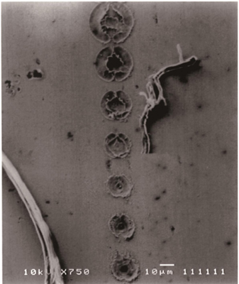
![46.9 nm laser ablation on brass surface[40]](/richHtml/zgjg/2024/51/7/0701009/img_01.jpg)
Fig. 1. 46.9 nm laser ablation on brass surface[40]
![ZEMAX software simulation and Si surface ablation results of a 46.9 nm laser focused by a cylindrical mirror[42]](/richHtml/zgjg/2024/51/7/0701009/img_02.jpg)
Fig. 2. ZEMAX software simulation and Si surface ablation results of a 46.9 nm laser focused by a cylindrical mirror[42]
Fig. 3. Toroidal mirror focused 46.9 nm laser ablation formed on the Si surface[43]
Fig. 4. Ablation hole with the diameter of 82 nm obtained at 7 μm from the focal plane of FZP[45]
Fig. 5. Schematic diagram of the wavefront splitting achieved by the Loe mirror[46]
Fig. 6. Nanopits and nanodots based on interferometric etching[47]. (a) Nanopits; (b) nanodots
Fig. 7. Schematic diagram of the tubular optical element[49]
Fig. 8. Focused interference etching by 46.9 nm laser[49]
Fig. 9. Periodic image self-healing based on Talbot effect[50]. (a) Mask; (b) etched result
Fig. 10. Ablation rate of the three kinds of materials by 46.9 nm laser at different fluences and pulse numbers[54]
Fig. 11. Schematic diagram of Faraday cup detection of 46.9 nm laser-induced plasma[53]
Fig. 12. Electronic signals detected by Faraday cup[53]
Fig. 13. Schematic representation of a Langmuir probe detecting 46.9 nm laser-induced plasma[63]
Fig. 14. Nanoparticles generated by monolayer graphene-assisted 46.9 nm laser irradiation[71]. (a) Cross-section depth; (b) ablation of the bare glass substrate; (c) graphene-assisted ablation of the glass substrate
Fig. 15. LIPSS formed by 46.9 nm laser in the ablated region of PMMA[72]. (a) Two-dimensional ablation pattern; (b) three-dimensional ablation pattern
Fig. 16. LIPSS-II formed by 46.9 nm laser in the ablated region of PMMA[73]
Fig. 17. LIPPS induced by single- and multi-shot 46.9 nm laser pulses in the BaF2 ablation region[74]. (a) Ablation induce by single laser pulse; (b) ablation induced by multiple pulses laser
Fig. 18. Periodic structural morphology at the boundary of the BaF2 ablation region[75]. (a) Ablation area; (b) edge of the ablation area
Fig. 19. Relationship between the period of micro-nano structures formed within the BaF2 ablation region and laser energy density[76]. (a) 230 mJ/cm2; (b) 30 mJ/cm2; (c) 15 mJ/cm2
Fig. 20. Schematic diagram of the 46.9 nm laser mass spectrometer[79]
Fig. 21. High-resolution three-dimensional mass spectrometry imaging achieved by 46.9 nm laser mass spectrometer[80]. (a) m/z=70.1; (b) m/z=81.1; (c) confocal microscopy image of the sample
Fig. 22. Radiation dose of 46.9 nm laser in relation to SSB and DSB yields of DNA molecules[87].(a) Radiation dose in relation to SSB yield; (b) radiation dose in relation to DSB yield
Fig. 23. 46.9 nm laser Gabor holographic device diagram and side view[89]
Fig. 24. Schematic diagram of 46.9 nm laser Fourier transform holographic imaging device[91]
Fig. 25. Schematic diagram of 46.9 nm laser diffraction microscope device[92]
Fig. 26. Diffraction patterns and reconstructed images before and after correction[92]
Fig. 27. Schematic diagram of 46.9 nm laser full-field microscope device[93]
Fig. 28. Nano tip single shot image and oscillation in the period[93]
| |||||||||||||||||||||||||||||
Table 1. Decay depth of 46.9 nm and 157 nm laser in PTFE, PMMA and PI and the ablation rate of the three kinds of materials[54]

Set citation alerts for the article
Please enter your email address


