Jun Zhang, Tian Jiang, Tong Zhou, Hao Ouyang, Chenxi Zhang, Zheng Xin, Zhenyu Wang, Xiang’ai Cheng, "Saturated absorption of different layered Bi2Se3 films in the resonance zone," Photonics Res. 6, C8 (2018)
Copy Citation Text
Here, we used the micro P-scan method to investigate the saturated absorption (SA) of different layered continuous films. Through resonance excitation, first, we studied the influence of the second surface state (SS) on SA. The second SS resonance excitation (~) resulted in a free carrier cross section that was 4 orders of magnitude larger than usual. At the same time, we found that the fast relaxation process of the massless Dirac electrons is much shorter than that of electrons in bulk states. Moreover, the second SS excitation resonance reduced the saturation intensity. Second, we studied the effect of the thickness on the SA properties of materials. The results showed that the saturation intensity was positively correlated to the thickness, the same as the modulation depth, and the thicker the film was, the less the second SS would influence it. This work demonstrated that by using as a saturable absorber through changing the thickness or excitation wavelength, a controllable SA could be achieved.
In the last few years, much research has focused on three-dimensional topological insulators (TIs) because of their special bulk insulating states and robust metallic surface state (SS) [1–5]. Actually, the metallic SS (including the first SS and the second SS), which is the origin of topological protection, suppression of backscattering, and helical spin texture, is significant for spintronics applications [6].
Recently, the nonlinear optics community has also paid attention to this novel material. Many groups focus on the nonlinear absorption and the optical Kerr effect. They want to explore applications such as saturable absorbers [7] and all-optical switching [8,9] based on this sort of quantum material. Because of the narrow bandgap and special electronic structure, TIs can achieve broadband saturated absorption (SA) and narrow pulse-width modulation. For instance, Ref. [10] reported a diverse soliton operations fiber laser using as a saturable absorber whose modulation depth is 9.8% and measured pulse width is 1.26 ps. Nevertheless, generally, previous nonlinear absorption research takes TIs as a mediocre quasi-semiconductor. There needs to be a detailed investigation about the influence from the special electronic structure, especially the SS (can be occupied by the massless Dirac electrons), which is essential for understanding the whole nonlinear absorption process of TIs. Last but not least, TIs are such novel materials that the Dirac cone cannot form unless there are more than five (at least six) layers [6]. Therefore, layer-dependent nonlinear absorption is also needed.
Furthermore, the most powerful instrument for characterizing the band structure of TIs is angle-resolved photoemission spectroscopy (ARPES) [11]. This system can precisely obtain the density of states and band structure of samples. However, unlike the condensed matter physics community, other research fields usually only need rough information such as band position and local band structure. ARPES is too costly for them. In fact, three-order nonlinear optical absorption (NOA) as a macroscopical reflection of density of states and carrier activity, to some extent, can also embody the features of band structure. For example, saturable absorption, as one of the most typical nonlinear absorption effects, is mainly caused by the state filling and Pauli exclusion principle [12–15]. At the same time, because of energy and angular momentum matching, for a specific single photon, only the corresponding energy band can respond. That means the SA properties of materials reflect the level of difficulty to fill the state of a certain band. Therefore, it is valuable to use nonlinear absorption measurement to assist the characterization of band structure, which has been reported less often until now.
Sign up for Photonics Research TOC. Get the latest issue of Photonics Research delivered right to you!Sign up now
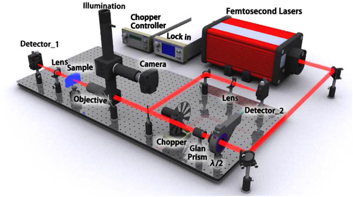
Generally, NOA is measured by open-aperture Z-scan (OAZ) [16,17]. OAZ, as a convenient method to measure the three-order NOA, is low cost and easy to operate [18–20]. But traditional OAZ systems cannot measure tiny samples precisely because of the relative displacement between samples and laser. For microsamples, instead of OAZ, the open-aperture micro P-scan is needed (as shown in Fig. 1) [21].
Figure 1.Schematic diagram of the open-aperture micro P-scan system. A 1/2 wavelength slide and a Glan prism are used to modulate the intensity of the laser. The chopper modulates the laser from 1 kHz to 500 Hz. An IDS camera and a Mitutoyo near-infrared objective lens (, ) are used to build up the video microscope system (VMS). Two lock-in amplifiers are used to measure the power of the laser.
In this paper, we studied the SA of the unoccupied electronic structure in different layered continuous films through the micro P-scan method in the resonance region (600, 700, 800 nm) (laser repetition rate 1 kHz, pulse width , waist diameter μ). Through model fitting, we found that the massless Dirac electrons played an important role in the nonlinear absorption process under low intensity excitation (below ). Specifically, the electronic band around 2.07 eV had a large , while the others did not, which could be used to distinguish the second SS. Moreover, we found that second SS resonance could improve the response speed and reduce the saturation intensity of . In addition, we found that thin possessed low saturation intensity, while thick had high modulation depth. If we control both the excitation wavelength and the thickness of material at the same time, can be a proper candidate for a parameter tunable saturable absorber that achieves broadband absorption and miniaturization.
2. CHARACTERIZATION
The samples used in this research were acquired by molecular beam epitaxy (MBE). MBE growth was performed in a custom-made MBE system with a base pressure of . The substrates were prepared by heating to 600°C for 2 h and 800°C for 1 h by indirect heating in an MBE chamber. High-purity elemental Bi (99.9999%) and Se (99.999%) were thermally evaporated from Knusden cells. To ensure stoichiometric samples were grown, a high Se/Bi flux ratio of was used, while the substrate temperature was kept around 200°C measured by an infrared pyrometer. All MBE growth was followed by 10 min of annealing, with growth temperature maintained and all evaporators shut off. The RH30OM reflection high-energy electron diffraction (RHEED) measurement system was used to monitor the crystal quality of the thin films during growth.
Figure 2(a) shows that the lattice constant of on substrate is 4.194 Å. To characterize the surface profile of 10 QL (1 QL ) , atomic force microscopy (AFM) was used, as shown in Fig. 2(b). In the AFM figure, it was smooth enough that would maintain its intrinsic properties. Furthermore, Raman spectroscopy was also measured. In Fig. 2(c), three intensity peaks () were around , , and , which ensured the sample’s purity [11]. Finally, the linear absorption spectrum (LAS) was used to roughly locate the resonance region. As shown in Fig. 2(d), the peaks of absorption are around 600 nm. With the layer increasing, there is a redshift of peaks because of the quantum confinement effect.
Figure 2.Characterization of the continuous layered films. (a) Streaks of on substrate. The lattice constant values of the epitaxy film is 4.194 Å. (b) AFM profile of layered film. (c) Raman spectra of these five different quintuple layer (QL) films. (d) LAS of different QL films. The peak absorption wavelengths of different QLs are 506, 572, 616, 626, and 650 nm.
The open-aperture micro P-scan technique was employed in our research, which was an efficient method for obtaining the nonlinear coefficient. Here, representative data are shown in Fig. 3. Comparing Figs. 3(a), 3(b), and 3(c), we qualitatively come to two conclusions: the damage threshold increased with thickness, while the nonlinear effects were positively correlated with thickness. As for quantitative analysis, rigorous mathematical deduction was needed.
Figure 3.Transmission spectra induced by the 600, 700, and 800 nm lasers. (a), (c), (e) Summary curves of different films (2 QL, 4 QL, 8 QL, 10 QL, 16 QL) excited by 600, 700, and 800 nm lasers; (b), (d), (f) fitting curves of (16 QL) fitted by different models excited by 600, 700, and 800 nm lasers.
Based on the Lambert–Beer law, the attenuation of a light beam passing through an optical medium can be described as [12]where is the propagation distance in the sample, and is the total absorption coefficient.
In fact, contains linear absorption and nonlinear absorption. According to different situations, nonlinear absorption terms have different forms. As we have adopted resonance excitation, first, we take SA based on a two-level model into consideration. The equation is shown as follows [13]: where is the linear absorption coefficient, and is the saturation intensity of .
We combine Eqs. (1) and (2) to fit the experimental data. Nevertheless, as shown in Figs. 3(b), 3(d), and 3(f) (the blue fitting line), all data cannot be fitted well using this model. So, it is reasonable to believe that other kinds of nonlinear absorption occur. So, we introduce the polarization model.
The polarization model ignores nonlinear absorption more than the three-order model does because during the whole experiment, the incident light intensity is below , which is very low. The mathematical expression is where and are the three-order saturated coefficient and three-order reverse-saturated coefficient, respectively. is the total three-order nonlinear absorption coefficient. In detail, comes from the Pauli exclusion principle caused by the state filling effect. originates from multiple interaction between photons and carriers (such as two-photon absorption and excited-state absorption). Furthermore, is negative, which reduces absorption, while is the opposite.
The fitting results show that the is negative, which means the absolute value of is larger than . Then, considering that the laser intensity is very low, the probability of multiple interactions can be ignored. So, here we deduce , and only comes from the single-photon nonlinear effect. Based on the inference, we take the homogeneous and inhomogeneous broadening model into consideration. The revised formula is as follows [22–26]: where is the intrinsic nonlinear absorption coefficient and is the saturation intensity of . The HSA model and In_HSA model are homogeneous and inhomogeneous broadening systems, respectively.
Combining Eq. (1) with Eqs. (5) and (6) to fit the data, we find that the HSA model is much more suitable [the purple fitting line in Figs. 3(b), 3(d), and 3(f)], especially compared with the In_HSA model. But the HSA model is not good enough. As shown in Fig. 3(b), when the intensity is below , the fitting is imprecise. This phenomenon is very significant when the wavelength of the laser is 600 nm. According to this, it is reasonable to guess that the accumulative nonlinearity, for example, the free-carrier absorption (FCA), plays an important role in it. Hence, we modify the nonlinear transmittance formula [integral of Eq. (1)] and put forward a revised model as follows [27]: where is critical fluence, ( is the FCA cross section), and is photon fluence. Moreover, is the transmission formula coming from the integral transformation of Eq. (1), based on the HSA model. Finally, we need Eq. (9) to get the modulation depth [28]: where MD is the modulation depth. and are the maximum and minimum transmission rates.
B. Discussion
1. Large FCA Cross Section Coming from the Second SS
Of all of these models, the HSA + FCA model is the best one for fitting no matter whether the laser wavelength is 600, 700, or 800 nm. Importantly, only when induced by 600 nm, the sample exhibits a large FCA cross section (shown in Table 1). On average, induced by a 600 nm laser is 4 orders larger than when induced by 700 and 800 nm.
Wavelength (nm)
Layer (QL)
600
700
800
2
N.A
0.922
0.189
4
1.61
0.338
0.125
8
42.69
0.122
0.0978
10
276.73
0.0948
0.0770
16
7214.54
0.0913
0.0773
Table 1. FCA Cross Section of Films under Different Excitation Wavelengths (, )
Based on the above methods, we draw the key parameters into Fig. 4 and list them as Tables 1–4. From Fig. 4(d), we can notice that the 600 nm laser induces the largest FCA cross section, while the FCA cross section induced by 700 and 800 nm lasers is near zero. Moreover, this phenomenon will be sharper when the layer increases. For , its thickness is a key parameter. According to previous studies, when there are more than six layers of , the continuous SS appears, filled with massless Dirac electrons, which are easy to excite and have a high mobility [6]. At the same time, the bulk state is insulating. When we use different lasers to irradiate the sample, the ground state of the induced electrons is the same. But their excited state is relative to the photon energy. If electrons are excited to the second SS, it is very likely for them to keep absorbing photons and transmit to a higher level. Considering the large FCA cross section induced by the 600 nm laser, we have reason to believe electrons are excited to the second SS. That means the second SS is . The electron transition process is shown in Fig. 4(a). Taking the blueshift of the energy band caused by the quantum confinement effect into account, this result is well matched with Ref. [4]. The conclusion proves that the second SS possesses a large FCA cross section that can be used to roughly locate the Dirac cone. But further study of this method is still needed.
Figure 4.(a) Diagrammatic sketch of carrier transition in . Different from linear excitation, nonlinear excitation will pump the electrons from the valence band to the conduction band rather than from the Fermi level. (b), (c), (d) Saturation intensity/intrinsic nonlinear absorption coefficient/FCA cross section of with different thickness excited by 600 to 800 nm lasers, where is the intrinsic nonlinear absorption coefficient and is the saturation intensity of .
2. Fast Relaxation in the Second SS Is Quicker than in Bulk States
Next, we analyzed an abnormal phenomenon. For given material, reflects the intrinsic capability of SA. The greater the absolute value of is, the more easily the material becomes saturated. However, from Fig. 4(c), we find that the second SS is hard to fill up, although its density of states is very low [4]. Considering the pulse width of the laser is around 65 fs, we infer this is because the fast relaxation process of electrons in the second SS is very quick. Specifically, according to previous reports, the density of states increases when the bands are away from the Dirac point, which indicates that the second SS has the shortest fast relaxation time. To verify our conjecture, we conducted a wide spectrum pump probe measurement. As shown in Fig. 5, the whole fast relaxation time rises from 0.64 to 0.83 ps when the excitation wavelength increases from 600 to 660 nm. Since the process in the first 65 fs has the same trend, just like the whole process, the pump probe results confirmed our conjecture.
Figure 5.Relaxation process of carriers in 16-layer films excited by 600–660 nm lasers. When the photon energy descends from (600 nm) to (660 nm), the fast relaxation time () of carriers corresponding to the band increases from 0.64 to 0.83 ps.
In this section, we discuss the performance of as a saturable absorber. As for application, there are four key parameters we should mention: they are the size, saturation intensity, modulation depth, and damage threshold intensity. For nanosheets grown by MBE, the size ranges from a few microns to millimeters, which is suitable for the integrated optical chips and microlasers, making up for the shortage of traditional saturated absorbers.
Next, the saturation intensity. For low power lasers, for example, most fiber lasers, saturation intensity represents the difficulty of reaching saturation. From Fig. 4(b) and Table 2, we can see that the saturation intensity is positively correlated with the thickness of the sample, while the trend is the same when the excitation wavelength increases from 600 to 800 nm. That means a few-layer or the second SS resonance excitation reaches a low saturation intensity.
And then, the modulation depth. Generally, the smaller the modulation depth is, the better the mode locking self-starting is. The larger the modulation depth is, the narrower the pulse width will be. From Table 4, we could conclude that there is a positive correlation between thickness and modulation depth, which means layered films can achieve tunable modulation depth by controlling the thickness. Even the maximum modulation depth is less than 1 dB, good for making a saturable absorber [28].
In fact, the performance of a saturable absorber is not determined by a single parameter. Not only this, but also in the specific application process, it is often limited by the structure of the laser. Based on the Ginzburg–Landau equation, we simulated the influence of modulation depth and saturation intensity on a positive astigmatic fiber laser. We found that with thin , it is easy to achieve high single-pulse energy and high-energy soliton pulse output, while with thick , it is likely to get a narrow pulse width. At the same time, the second SS resonance excitation is a better choice for a high single-pulse energy and narrow pulse-width laser.
Next, we deal with the damage threshold intensity. Usually, there are two ways to damage the saturable absorber—thermal accumulation and electron avalanche. The thermal conductivity of is not as good as that of graphene, and under the high intensity SS resonance excitation, the massless Dirac electrons easily cause an electron avalanche. So, the damage threshold intensity of is low. As shown in Figs. 3(a), 3(b), and 3(c), the few-layer is more easily damaged than the thicker, while the second SS resonance excitation reduces the damage threshold. A more detailed discussion needs a series of experiments using different repetition rates and different pulse-width lasers, which we will do in the future.
Finally, when comparing the parameters of different layered films in Tables 1–4, we find that the thicker the material is, the less affected the films are by the second SS resonance excitation.
4. CONCLUSIONS
In conclusion, SA of different layered films synthesized by MBE is measured by micro P-scan in the resonance region. We found that the second SS possessed a large FCA cross section (4 orders higher than in the bulk state), which could be used to locate the second SS. And the second SS resonance excitation could reduce the saturation intensity. At the same time, the results from different layered films showed that the saturation intensity is positively correlated with the thickness, the same as the modulation depth. The thicker the film is, the less influenced it will be by the second SS. This work provides a deep study of the saturable absorber, which is important for laser design.
Acknowledgment
Acknowledgment. We really appreciate Yizhen Sui and Yuxiang Tang’s help, especially their efforts on the Raman and PL measurement.
[22] N. Dong, Y. Li, S. Zhang, N. McEvoy, R. Gatensby, G. S. Duesberg, J. Wang. Saturation of two-photon absorption in layered transition metal dichalcogenides: experiment and theory. ACS Photon., 5, 1558-1565(2018).