• Acta Physica Sinica
  • Vol. 68, Issue 4, 048801-1 (2019)
Sheng-Sheng Zhao1、2、3、4, Yu-Zeng Xu1、2、3、4, Jun-Fan Chen1、2、3、4, Li Zhang1、2、3、4, Guo-Fu Hou1、2、3、4、*, Xiao-Dan Zhang1、2、3、4, and Ying Zhao1、2、3、4
Author Affiliations
  • 1Institute of Photoelectronic Thin Film Devices and Technology of Nankai University, Tianjin 300350, China
  • 2Key Laboratory of Photoelectronic Thin Film Devices and Technology of Tianjin, Tianjin 300350, China
  • 3Engineering Center of Thin Film Photoelectronic Technology of Ministry of Education, Tianjin 300350, China
  • 4Sino-Euro Joint Research Center for Photovoltaic Power Generation of Tianjin, Tianjin 300350, China
  • show less
    DOI: 10.7498/aps.68.20181991 Cite this Article
    Sheng-Sheng Zhao, Yu-Zeng Xu, Jun-Fan Chen, Li Zhang, Guo-Fu Hou, Xiao-Dan Zhang, Ying Zhao. Research progress of crystalline silicon solar cells with dopant-free asymmetric heterocontacts[J]. Acta Physica Sinica, 2019, 68(4): 048801-1 Copy Citation Text show less
    Passivated contact solar cell structure and carrier transport mode[13].钝化接触太阳电池结构及载流子输运方式[13]
    Fig. 1. Passivated contact solar cell structure and carrier transport mode[13]. 钝化接触太阳电池结构及载流子输运方式[13]
    energy band structure diagram.能带结构示意图
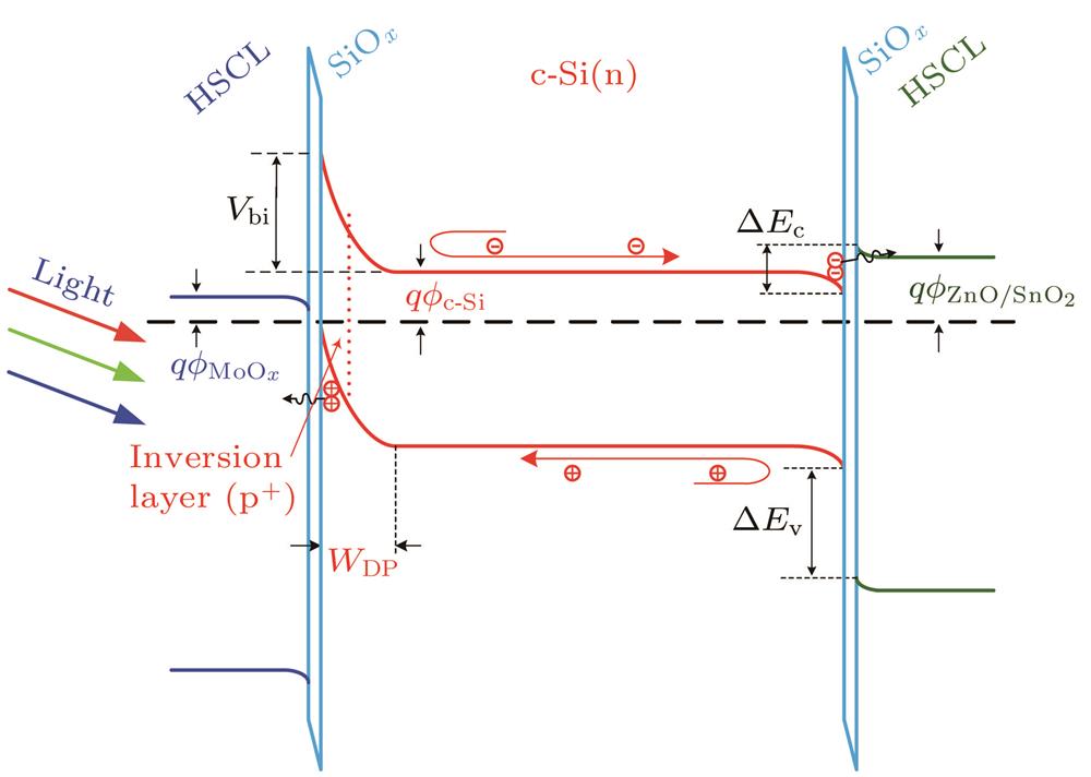
    Fig. 2. energy band structure diagram.能带结构示意图
    Schematics of the NiO/c-Si/TiO2 solar cell structure[9].NiO/c-Si/TiO2结构太阳电池示意图[9]
    Fig. 3. Schematics of the NiO/c-Si/TiO2 solar cell structure[9]. NiO/c-Si/TiO2结构太阳电池示意图[9]
    (a) Schematics of the MoOx/n-Si heterojunction solar cell structure; (b) cross section imaged by scanning electron microscopy[16].(a) MoOx/c-Si异质结太阳电池结构的示意图; (b)通过扫描电子显微镜成像的横截面图[16]
    Fig. 4. (a) Schematics of the MoOx/n-Si heterojunction solar cell structure; (b) cross section imaged by scanning electron microscopy[16]. (a) MoOx/c-Si异质结太阳电池结构的示意图; (b)通过扫描电子显微镜成像的横截面图[16]
    Schematics of the full back contact solar cell structure[10].全背接触结构的太阳电池示意图[10]
    Fig. 5. Schematics of the full back contact solar cell structure[10]. 全背接触结构的太阳电池示意图[10]
    (a)BackPEDOT solar cell front; (b) schematic cross-section of the BackPEDOT solar cell[39].(a)BackPEDOT太阳电池正面; (b)BackPEDOT太阳电池横截面示意图[39]
    Fig. 6. (a)BackPEDOT solar cell front; (b) schematic cross-section of the BackPEDOT solar cell[39]. (a)BackPEDOT太阳电池正面; (b)BackPEDOT太阳电池横截面示意图[39]
    The structure of MLBC solar cell[11].MLBC太阳电池结构[11]
    Fig. 7. The structure of MLBC solar cell[11]. MLBC太阳电池结构[11]
    Silicon heterojunction cell structure using MoOx as hole selective contact; (a) n-a-Si:H as electron selective contact; (b) ZnO:B as electron selectivecontact[47].使用MoOx作为空穴选择性接触的硅异质结电池结构 (a)n-a-Si:H作为电子选择性接触; (b)ZnO:B作为电子选择性接触[47]
    Fig. 8. Silicon heterojunction cell structure using MoOx as hole selective contact; (a) n-a-Si:H as electron selective contact; (b) ZnO:B as electron selectivecontact[47]. 使用MoOx作为空穴选择性接触的硅异质结电池结构 (a)n-a-Si:H作为电子选择性接触; (b)ZnO:B作为电子选择性接触[47]
    Characteristics of silicon heterojunction cells with MoOx as hole selective contact, n+-a-Si:H and ZnO:B as electron selective contact respectively: (a) J-V curve; (b) EQE curve[47].采用MoOx作为空穴选择性接触, 分别n+-a-Si:H和ZnO:B作为电子选择性接触的硅异质结电池特性 (a)J-V曲线; (b)EQE曲线[47]
    Fig. 9. Characteristics of silicon heterojunction cells with MoOx as hole selective contact, n+-a-Si:H and ZnO:B as electron selective contact respectively: (a) J-V curve; (b) EQE curve[47]. 采用MoOx作为空穴选择性接触, 分别n+-a-Si:H和ZnO:B作为电子选择性接触的硅异质结电池特性 (a)J-V曲线; (b)EQE曲线[47]
    (a) The image of an as-deposited MoOx film on c-Si; (b) the image of the MoOx and c-Si interface; (c) cross-sectional STEM image for the region of the EDS line scan; (d) compositional distribution of each element measured using the EDS line scan showing a thinSiOx layer formed between the MoOx and the c-Si[35].(a)在c-Si上沉积MoOx薄膜的横截面图像; (b)MoOx和c-Si的交界处图像; (c)EDS线扫描区域的横截面STEM图像; (d)使用EDS线测量每个元素的组成分布, 显示在MoOx和c-Si之间形成薄的SiOx层[35]
    Fig. 10. (a) The image of an as-deposited MoOx film on c-Si; (b) the image of the MoOx and c-Si interface; (c) cross-sectional STEM image for the region of the EDS line scan; (d) compositional distribution of each element measured using the EDS line scan showing a thinSiOx layer formed between the MoOx and the c-Si[35]. (a)在c-Si上沉积MoOx薄膜的横截面图像; (b)MoOx和c-Si的交界处图像; (c)EDS线扫描区域的横截面STEM图像; (d)使用EDS线测量每个元素的组成分布, 显示在MoOx和c-Si之间形成薄的SiOx[35]
    Device ArchitectureJsc/mA·cm-2Voc/mV FFEfficiency/%Reference(Year)
    MoOx/nc-Si/n a-Si:H 37.85806514.3Battaglia et al.[16](2014)
    MoOx/i a-Si:H/c-Si/i a-Si:H/n a-Si:H 38.6725.480.3622.5Jonas et al.[26](2015)
    p+-Si/p-c-Si/MoOx376167216.4Bullock et al.[43](2015)
    p+-Si/n-c-Si/TiO239.263979.119.8Yang et al.[44](2015)
    MoOx/a-Si:H(i)/c-Si/a-Si:H(i)/LiFx37.07716.473.1519.42Bullock et al.[8](2016)
    MoOx/ia-Si:H/nc-Si/ia-Si:H/n a-Si:H 39.471167.218.8Battaglia et al.[17](2016)
    V2Ox/c-Si/ n a-Si:H 34.460675.315.7Gerling et al.[15](2016)
    MoOx/c-Si/ n a-Si:H 34.158168.813.6Gerling et al.[15](2016)
    WOx/c-Si/ n a-Si:H 33.35776512.5Gerling et al.[15](2016)
    p+-Si/n-c-Si/SiO2/TiO239.56508020.5Yang et al.[45](2016)
    V2Ox /Au /V2Ox38.765175.4919.02Wu et al.[11](2017)
    p+-Si/n-c-Si/MgOx39.562880.620Wan et al.[46](2017)
    MoOx/i a-Si:H/c-Si/i a-Si:H/BZO 38.159972.716.6Wang et al.[47](2017)
    MoOx/a-Si:H(i)/c-Si/a-Si:H(i)/TiOx/LiF 38.470676.220.7Bullock et al.[32](2018)
    Table 1.

    Summary of Silicon Heterojunction Solar Cells Based on TMO Carrier Selective Contact.

    基于TMO载流子选择性接触的硅异质结太阳电池研究现状

    Sheng-Sheng Zhao, Yu-Zeng Xu, Jun-Fan Chen, Li Zhang, Guo-Fu Hou, Xiao-Dan Zhang, Ying Zhao. Research progress of crystalline silicon solar cells with dopant-free asymmetric heterocontacts[J]. Acta Physica Sinica, 2019, 68(4): 048801-1
    Download Citation